Improved vertical isolation of GaN-based high-voltage transistors for power electronics application
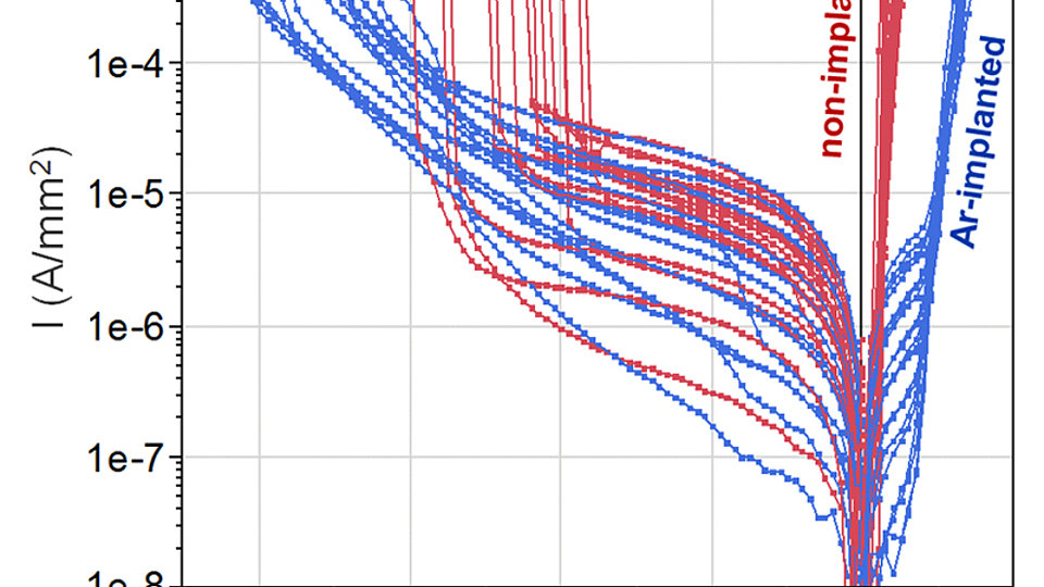
Fig. 1: Vertical leakage currents at various wafer positions with (blue) and without (red) n-SiC substrate implantation.
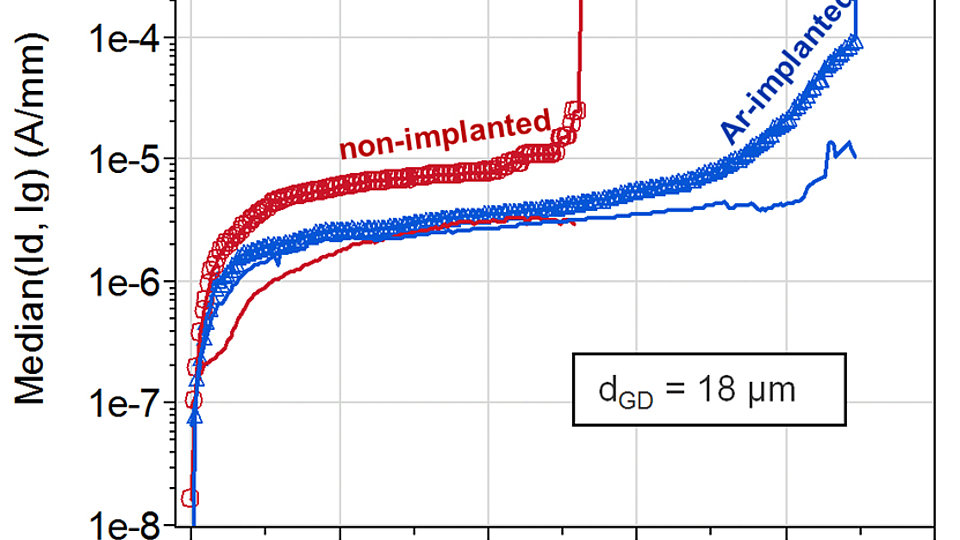
Fig. 2: Wafer median of the transistor off-state drain (open symbols) and gate (line) leakage currents.
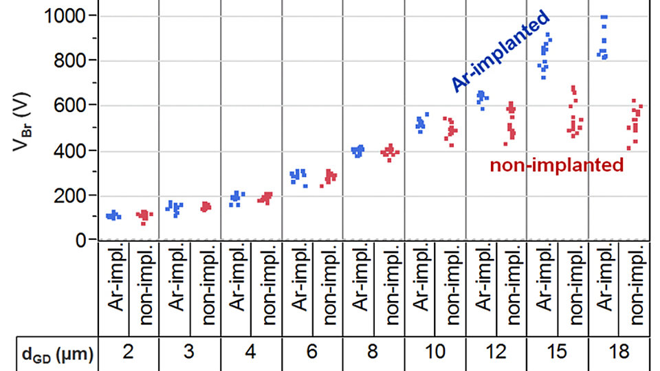
GaN-based high-voltage switching transistors enable compact and efficient power converters due to the low area-specific on-state resistance for a given blocking strength (RONA/ VBr) and the particular low switching losses. The breakdown strength of the AlGaN/GaN HFETs increases with the lateral gate-drain spacing dGD, typical values for the lateral blocking strength are 50 V/µm. More than 12 µm gate-drain separation is thus needed for 600 V device operation.
The semiconductor layers of AlGaN/GaN HFETs are grown with epitaxy on extrinsic substrates in the production process. Due to cost considerations, conductive substrates like n-type SiC and Si are preferred as compared to semi-insulating SiC. The thickness of the deposited GaN layers is limited to 3 - 5 µm due to the mechanical strain induced by heteroepitaxy. The required vertical blocking strength of the (Al)GaN layers is thus higher than the lateral blocking strength, since there is no voltage drop on the conductive substrate. The vertical leakage currents were studied on AlGaN/GaN heterostructures that are based on a 3 µm thick iron-doped GaN buffer. In fact, the vertical leakage current limits the blocking from drain to substrate to 80 V and from source to substrate to 400 V. As consequence, the device blocking strength is limited to 500 V for a floating substrate and does not further increase above a gate-drain separation of 10 µm.
Conductive n-SiC substrates were Argon-implanted prior to epitaxial GaN-layer growth at FBH to generate an insulating layer at the upper substrate surface. Transistor structures on these pre-implanted substrates showed reduced vertical leakage currents and the vertical blocking strength between drain and substrate is increased to 150 V and between source and substrate to 700 V. A direct comparison between identical transistors on implanted and non-implanted substrates demonstrated an increase of the breakdown strength from 500 V to 900 V. The breakdown voltage now also scales with the gate-drain separation above 10 µm distance.
Special attention was payed to the question if the modified substrate would change the growth of the GaN layers. But the quality of the semiconductor stack has not suffered from the pre-implanted substrates. A careful analysis of the static and of the dynamic electrical transistor parameters revealed identical characteristics. The GaN-layer reflection peaks from material x-ray analysis (HRXRD) showed no increased peak width for the layers grown on pre-implanted SiC. The defect density is thus not increased.
Publications:
O. Hilt, P. Kotara, F. Brunner, A. Knauer, R. Zhytnytska, J. Würfl, "Improved Vertical Isolation for Normally-off High Voltage GaN-HFETs on n-SiC Substrates", IEEE Trans. Electron Devices, DOI 10.1109/TED.2013.2259492, 2013.
P. Kotara, R. Zhytnytska, O. Hilt, E. Cho, F. Brunner, A. Thies, J. Würfl, "Vertical blocking voltage improvement of GaN HEMT structures on n-SiC by pre-epitaxial substrate implantation", accepted for publication, ECS Journal of Solid State Science and Technology, Vol. 2(8), pp. N3064-N3067, 2013.
FBH research: 05.07.2013


