Higher yield due to laser scribing used for the fabrication of cleaved facets of GaN-based laser diodes
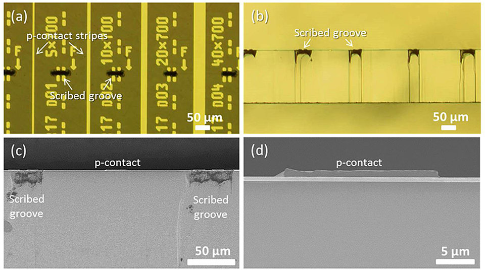
Fig. 1: Optical micrographs of the wafer surface after laser scribing (a) and of the cleaved facet (b). Cross sectional SEM micrographs of the cleaved facet with 10 µJ laser pulse energy and 500 mm/min laser scribing scan speed (c and d).
The fabrication of GaN-based laser diodes requires the formation of atomically smooth and parallel mirror facets. Cleaving is the preferred method to obtain such facets for most semiconductor systems, such as GaAs, since it allows the crystal to break along its natural cleavage plane. However, according to our experience, currently available c-plane GaN substrates still suffer from crystallographic imperfections which can act as starting points for an unwanted breaking of the wafer and can deflect a propagating cleavage plane from its ideal planar shape. Therefore, the classical diamond scribing/breaking technique often results in a low yield of the dicing process. We have studied in detail the laser machining of active GaN-based laser structures on c-plane GaN substrates using a UV laser and a skip-and-scribe approach in comparison to conventional diamond tip edge-scribing.
Processed broad area laser GaN wafers were first cleaved in 7.5 mm wide sections parallel to the contact stripes. Each section was then cleaved in bars with a cavity length of 1300 µm. Laser scribing was performed using a laser which emits at a wavelength of 355 nm and delivers 30 ns pulses with a repetition frequency of 20 kHz. Re-deposited material alongside the scribes was removed from the surface by wet-chemical etching. The dependence of the depth of the laser scribed groove on the scan velocity and the average pulse energy of the laser was investigated first. Whereas the depth of the laser scribed groove was found to be inversely proportional to the laser scan speed, the groove width increased with increasing laser pulse energy. Irrespective of the laser pulse energy, extended surface cracks were frequently generated by the laser scribing process but could be reduced by increasing the scan speed of the laser. As shown in Fig. 1(a), laser scribed grooves were segmented and placed inbetween the p-contact stripes of the lasers with a distance of 70 µm to the p-contact to minimize any possible collateral damage of the contact and related surface contamination from debris. The cleavage plane usually followed the line marked by the laser scribed grooves. Fig. 1(b) shows a typical cross section of the cleaved laser bars after laser scribing. The cleavage planes of laser scribed samples generally showed fewer terraces in comparison to those of diamond scribed samples. Moreover, most of the terraces are concentrated underneath the laser scribed grooves, as shown in Figs. 1(c) and (d).
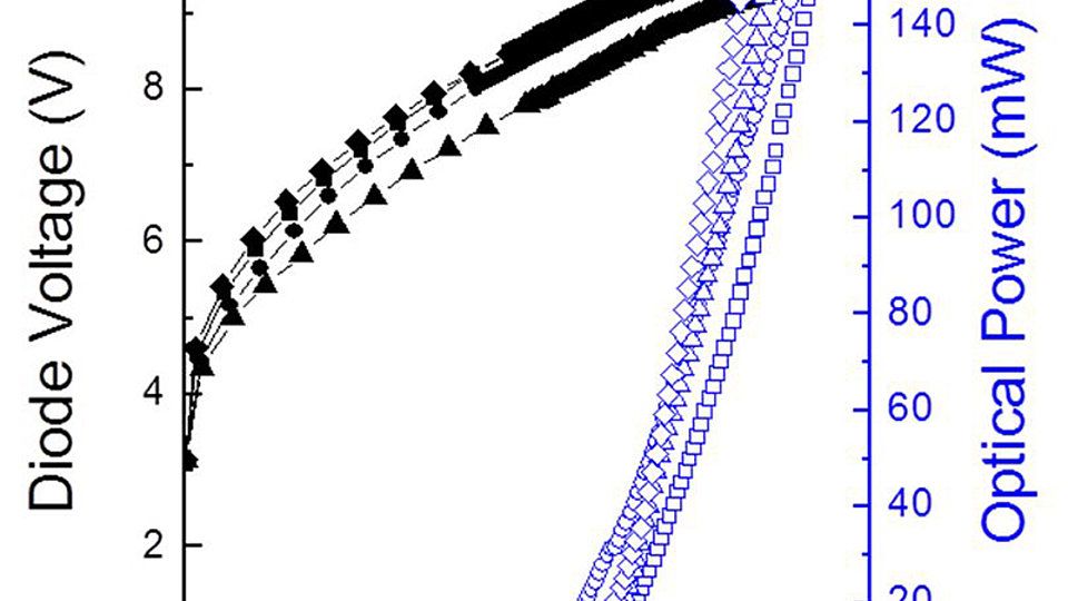
In comparison to the cleaving process with the diamond tip edge-scribing method, the laser skip-and-scribe method was found to increase the yield of properly broken laser bars by at least a factor of two. The light output power and voltage versus current (L-I-V) characteristics of the devices was measured on the laser bars, as shown in Fig. 2. The threshold current density, the threshold voltage, and the slope efficiency are very similar for the different scribing methods, i.e., there is no obvious impact of the scribing method on the electrical and the optical performance of the devices. In conclusion, the laser skip-and-scribe-method is a suitable method to fabricate reasonably smooth mirror facets within defined cleavage streets for GaN-based laser diodes on c-plane GaN substrate without negative impact on the device performance.

