Chip mounting technology for UV LEDs developed
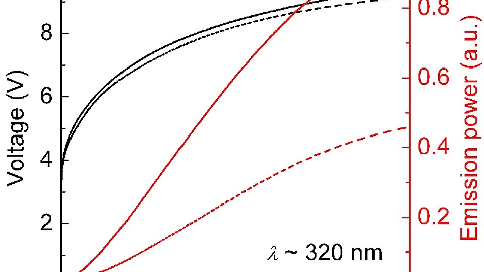
Fig. 2: Current-voltage-emission power characteristics of the LEDs measured on-wafer and after mounting.
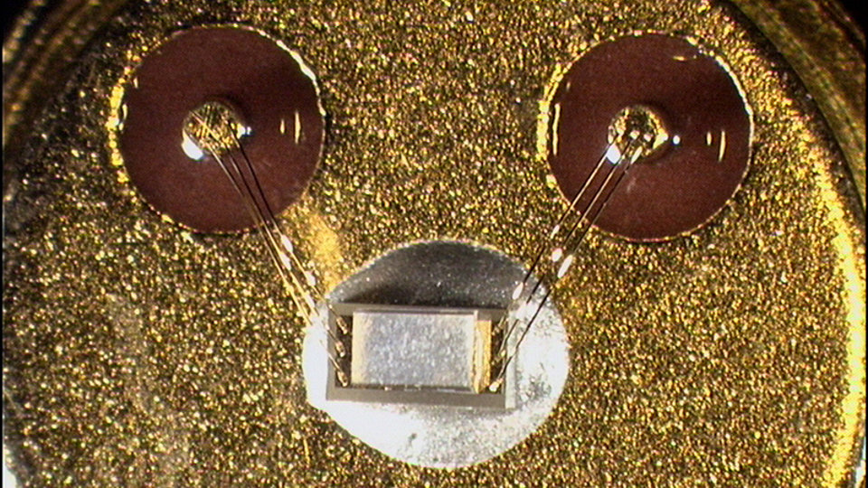
Particularly in view of the use in water disinfection, phototherapy and sensor technology, FBH develops efficient LEDs emitting UV-B light in the wavelength range 280 - 320 nm. So far, the work focussed on the optimization of the epitaxial structures by fabricating simple LED test structures and characterizing them through on-wafer measurements. Now, a technology has been developed which allows to fabricate LEDs as single chips and mount them on heat spreaders and into standard housings. For this purpose, the chip process has significantly gained in complexity. E.g. p- and n-contacts interdigitate, and they are separated from each other by an isolation layer to allow large-area soldering. Single chips of 0.6 mm x 1 mm size are obtained from wafers by laser scribing and subsequent cleaving. The chips are soldered on structured AlN heat spreaders in flip-chip geometry and glued and wire-bonded on a TO header. Fig. 1 is a top-view of an LED chip mounted in this manner.
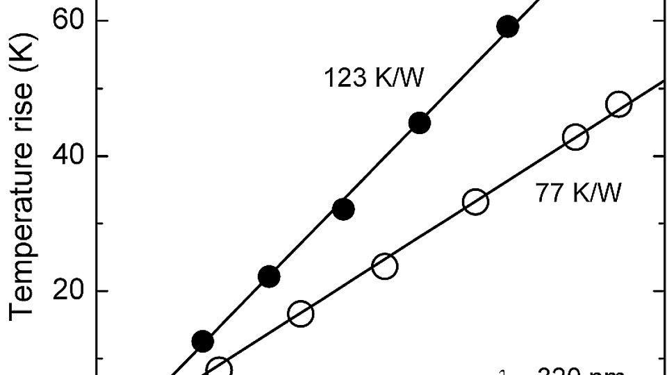
The feasibility of the mounting technology was proven with UV LEDs emitting at a wavelength of about 320 nm. Fig. 2 shows that the emission power of a mounted LED is larger by a factor of two in comparison to an on-wafer measurement. This effect can be attributed to the more efficient out-coupling of UV light through the side facets of the chip. Moreover, in case of the mounted LED, the heat is extracted more efficiently from the active area as demonstrated by measurements of the thermal resistance shown in Fig. 3. The available mounting technology enables FBH to supply evaluation models of its UV LEDs in a configuration which e.g. fit into UV LED modules used for water disinfection.
FBH research: 06.05.2011


