AlN layers with low dislocation density for UV LEDs
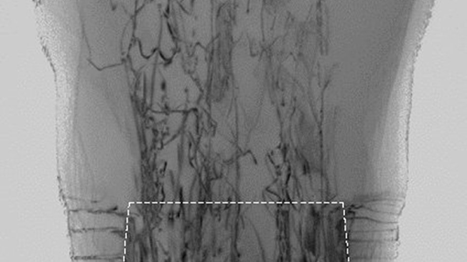
Fig. 1(a): Cross-sectional scanning electron microscope image of an AlN/sapphire stripe pattern before AlN overgrowth
Ultraviolet (UV) light can be used for a wide range of applications, as, for example, light with wavelengths around 265 nm for water purification. The Ferdinand-Braun-Institut develops light emitting diodes (LEDs) for the UV spectral range. However, for most applications the efficiency of these LEDs must be significantly improved. The devices base on the (Al,Ga)N material system which allows to adjust the emission wavelength between 210 nm and 365 nm by tuning the composition of this material. AlN layers on a sapphire substrate are used as underlying material due to their transparency in the UV range. As a consequence of the large lattice mismatch between (Al,Ga)N and the sapphire substrate, the epitaxy of (Al,Ga)N results in high threading dislocation densities in the range of 1010 cm-2. Dislocations dramatically reduce the efficiency of UV LEDs as carriers can recombine nonradiatively at these defects. Now, FBH managed to reduce the dislocation density of AlN by more than one order of magnitude by the epitaxial lateral overgrowth of patterned AlN layers.
For this purpose, AlN layers were deposited on sapphire by metal organic vapor phase epitaxy and subsequently structured into a stripe pattern with different stripe directions. Overgrowth with (Al,Ga)N resulted in compositional fluctuations [1]. Hence, overgrowth with binary AlN was employed. Fig. 1 shows the cross-sectional view of the stripe pattern before and after overgrowth. The AlN layer coalesced at a thickness of 2.5 µm. After overgrowth, stripes along the [1-100] direction show a uniform surface [2]. A transmission electron microscope image is depicted in fig. 2. The upper region of the overgrown AlN exhibits a significantly lower dislocation density than the primarily structured AlN layer. This method is therefore capable of reducing the dislocation density of AlN layers down to an average value of 109 cm-2. These layers are now used for further development of efficient UV LEDs at FBH.
Publications:
[1] V. Kueller, A. Knauer, F. Brunner, U. Zeimer, H. Rodriguez, M. Kneissl, M. Weyers, "Growth of AlGaN and AlN on patterned AlN/sapphire templates", J. Cryst. Growth, vol. 315, no. 1, pp. 200-203 (2011).
[2] V. Kueller, A. Knauer, U. Zeimer, H. Rodriguez, A. Mogilatenko, M. Kneissl, and M. Weyers, "(Al,Ga)N overgrowth over AlN ridges oriented in [1120] and [1100] direction", phys. stat. sol. C8, No. 7-8, 2022-2024 (2011).
FBH research: 29.07.2011


