75 mOhm / 600 V normally-off switching transistors on SiC and Si substrates
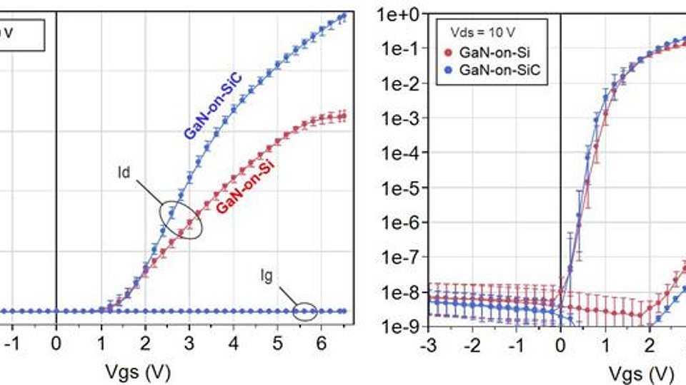
Fig. 2: Transfer characteristic (median, percentiles of wafer distribution) for GaN-on-Si and GaN-on SiC transistors with 3.2 mm gate width – linear (l.) and logarithmic (r.) representation
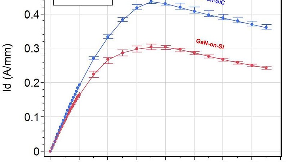
Fig. 3: On-state IV curve (wafer distribution, median, percentiles) for GaN-on-Si and GaN-on SiC transistors with 3.2 mm gate width
GaN-based high-voltage power switching transistors enable efficient power converters with increased power density due the low area-specific on-state resistance for a given blocking strength and the low switching losses. FBH transistors with GaN layers grown on SiC substrate have proven to outperform Si-based super-junction MOSFETs in terms of low switching energy (Eoss = 5 µJ at 400 V for RON = 65 mΩ) and low specific gate charge (QG x RON = 0.9 nCΩ). With an area-specific on-state resistance of RON x A = 0.66 Ωmm2 for the 600 V class, FBH GaN transistors are also competitive in terms of the required chip area. Currently, the major burden for market introduction for these new power semiconductor devices remains in the considerable costs, mainly due to expensive SiC substrates
Considerable progress in growing high-quality GaN layers on Si substrates with sufficient high-voltage isolation has been made recently. The cost-advantage of using silicon substrates with diameters up to 200 mm will help to substantially cut down the manufacturing costs, thus making the 600 V GaN technology competitive to Si-based devices also in terms of an often cited cost x (QG x RON) figure-of-merit.
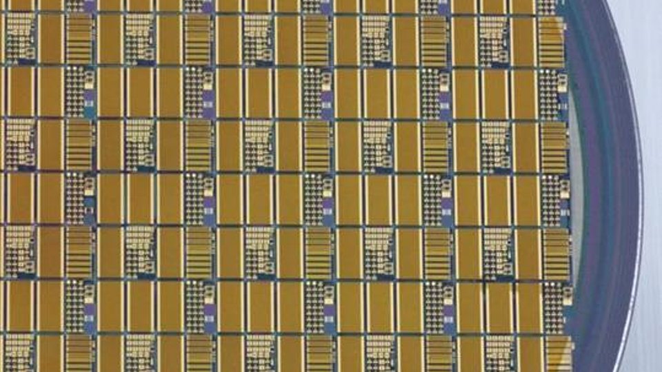
FBH has successfully transferred its 600 V technology for normally-off power switching transistors from the GaN-on-SiC platform to 4" GaN-on-Si wafers in the frame of the EU FP7 project HipoSwitch. Threshold voltage (Vth = 1.1 V), sub-threshold drain current, off-state drain leakage (10 nA/mm for 0 V gate bias) and on-state gate current (4-10 µA/mm for 5 V gate bias) are almost identical for both substrate types in on-wafer DC measurements of test transistors with 3.2 mm gate width.
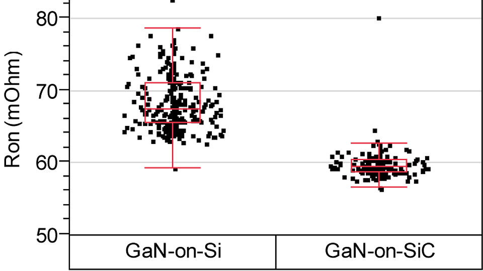
Major differences can be found for high power operation. The maximum drain current of the GaN-on-Si devices (Idsmax = 0.3 A/mm bei Vds = 7.5 V) is only 68% of the current of the GaN-on-SiC devices. The reduced current is only partially related to the 20% higher sheet resistance of the channel layer for the GaN-on-Si wafer. This is reflected in the differences of the on-state resistance (59 mΩ for GaN-on-SiC and 67 mΩ for GaN-on-Si transistors with 214 mm gate width) of the power switching transistors. The major contribution is found to be due to the increased channel temperature of GaN-on-Si transistor cells when an electric power of 7 W and more is dissipated on an active device area of 0.1 mm2. Here, SiC with its 3 times higher thermal conductivity as compared to silicon has a better potential to remove heat from the active device region. However, the impact of substrate type on the channel temperature will be less after substrate thinning, dicing, and packaging of the transistor chips.
Publications:
O. Hilt, E. Bahat-Treidel, F. Brunner, A. Knauer, R. Zhytnytska, P. Kotara, J. Wuerfl, "Normally-off GaN Transistors for Power Applications", J. Phys.: Conf. Ser., vol. 494, no. 012001 (2014).
O. Hilt, P. Kotara, F. Brunner, A. Knauer, R. Zhytnytska, J. Würfl, "Improved Vertical Isolation for Normally-off High Voltage GaN-HFETs on n-SiC Substrates", IEEE Transactions on Electron Devices, vol. 60, no. 10, pp. 3084-3090 (2013).
O. Hilt, E. Bahat-Treidel, F. Brunner, A. Knauer, R. Zhytnytska, P. Kotara, J. Wuerfl, "Normally-off GaN Transistors for Power Switching Applications", ECS Trans., vol. 58, no. 4, pp. 145-154 (2013).
FBH research: 14.08.2014


