65 mOhm / 600 V normally-off switching transistors for efficient energy conversion
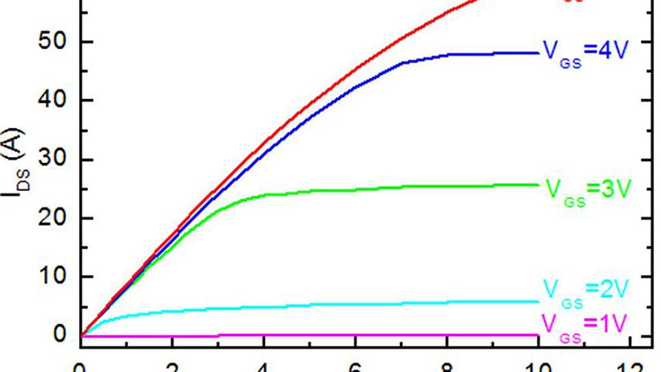
Fig. 1: Output characteristics of a normally-off 100 mOhm / 600 V GaN switching transistor with 134 mm gate width.
GaN-based high-voltage power switching transistors enable efficient power converters with increased power density. High converter switching frequencies can be realized with lateral GaN-based HFETs due the low area-specific on-state resistance for a given blocking strength and the low gate charge required for switching.
A normally-off transistor drive characteristic is usually required in power electronics systems: For this purpose, FBH has successfully developed GaN power switching transistors comprising a p-type GaN gate module to convert the GaN HEMT into a normally-off device. Static and dynamic electrical device characterizations have been performed on transistors with 134 mm gate width, featuring a chip size of 2.9 x 3.8 mm2. The devices have +1 V threshold voltage, 60 A pulse current, 100 mΩ on-state resistance and 600 V blocking voltage. The drain-source switching energy for this device for 400 V switching is 4 µJ and thus only 60 % of a similarly rated Si-based CoolMOS super-junction transistor. The required gate charge for switching was measured as QG = 6 nC. The resulting benchmark of QG x RON = 0.6 nCΩ, which is known as a measure for switching efficiency, is a factor 5 - 10 smaller than for Si-based MOSFETs with the same voltage rating. The targeted benefit in switching efficiency is thus proven for the FBH GaN-switching transistor technology.
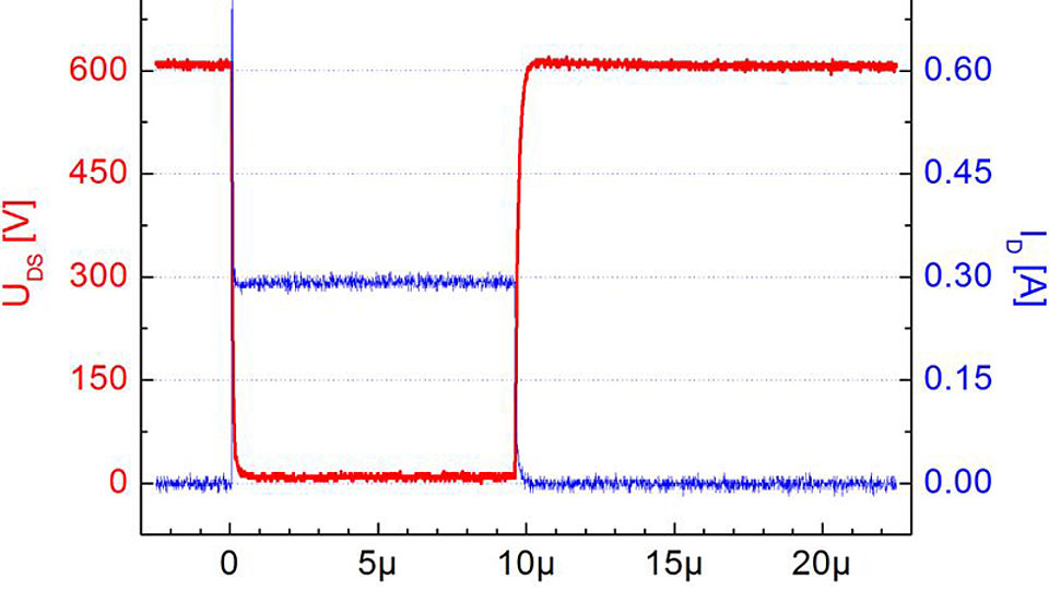
600 V / 0.3 A switching experiments have been performed with small test transistors with reduced gate width and 5 Ω on-state resistance and the current and voltage transients show only 70 ns rise time.
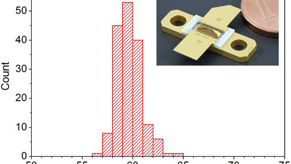
New 600 V devices have been fabricated using a novel layout that was optimized for more efficiently using the semiconductor area. 214.4 mm gate width was arranged on a 4.4 x 2.3 mm2 chip. These devices show very low on-state resistances of 65 mΩ or less. The area-specific on-state resistance was thus decreased by 40 % from RON x A = 1.09 Ωmm2 to RON x A = 0.66 WΩmm2. Less chip area is required for this FBH GaN transistor as compared to similarly rated 600 V Si-based super junction MOSFETs, featuring typically RON x A = 1-3 Ωmm2. This example demonstrates that efficient use of the chip area is also possible for the lateral design of GaN transistors. Actually, it can compete with the vertical design of Si-based transistors.
Publications:
O. Hilt, P. Kotara, F. Brunner, A. Knauer, R. Zhytnytska, J. Würfl, "Improved Vertical Isolation for Normally-off High Voltage GaN-HFETs on n-SiC Substrates", IEEE Transactions on Electron Devices, vol. 60, no. 10, pp. 3084-3090 (2013).
O. Hilt, E. Bahat-Treidel, F. Brunner, A. Knauer, R. Zhytnytska, P. Kotara, J. Wuerfl, "Normally-off GaN Transistors for Power Switching Applications", ECS Trans., vol. 58, no. 4, pp. 145-154 (2013).
N. Badawi, O. Hilt, E. Bahat-Treidel, S. Dieckerhoff, J. Würfl, "Switching Characteristics of 200 V Normally-off GaN HEMTs", Int. Exhibition and Conf. for Power Electronics, Intelligent Motion, Renewable Energy and Energy Management (PCIM Europe), Nuremberg, ISBN 978-3-8007-3505-1, pp. 319-324, (2013).
FBH research: 29.04.2014


