500 V switching of GaN HFETs
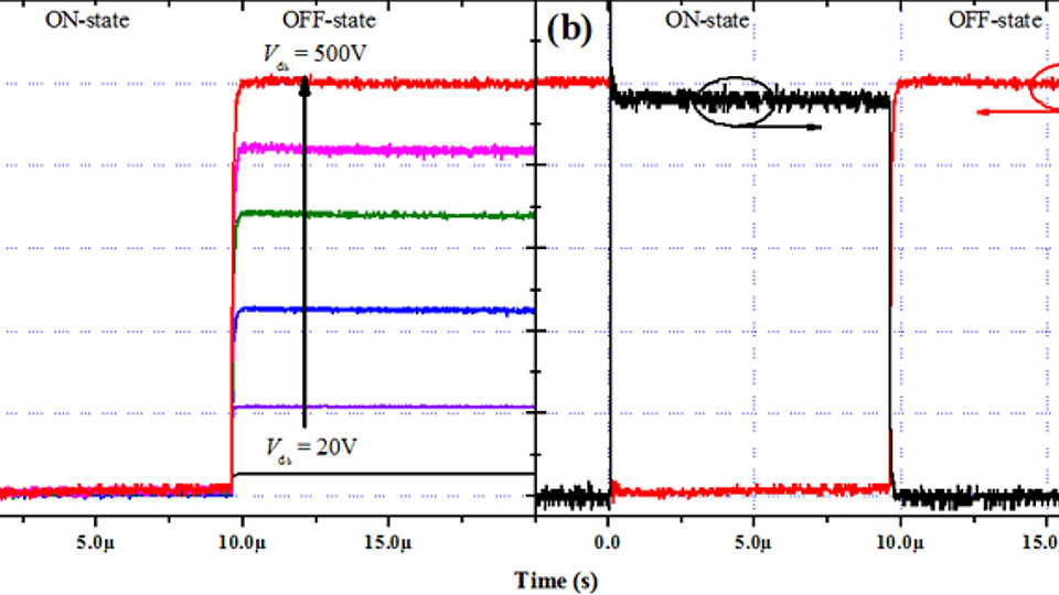
Fig. 2: Switching characteristics of a packaged test device with 2.1 mm gate width and 15 µm gate-drain separation. VGS is switched from 5 V (OFF state) to +1 V (ON state) and back after 10 µs. (a) ON and OFF state drain bias characteristics from Vds>/sub> = 20 V to 500 V, (b) 500 V / 0.5 A current and voltage switching transients.
Targets for next generation electronic power converters are – besides increased efficiency – reduced size in both weight and volume. Technically, such features are achievable by increasing the switching frequency, which allows the use of more compact passive components such as capacitors and inductors in the converter system. The introduction of GaN-based transistors with their particularly low switching losses will enable the high switching frequencies without penalty in system efficiency.
GaN‑based high‑voltage switching transistors show a low area‑specific on‑state resistance along with a low gate capacitance. However, they still suffer from an increase of the on‑state resistance when switching from high voltages, Ron_Dyn - which has been found to increase by orders of magnitude when switching from off‑state bias higher than 200 V. This increase indicates a carrier concentration reduction in the transistor channel originating from trap states in the semiconductor material. Such trap states are result of insulation doping of the grown GaN layers, but also of their structurally related defect density. The increased dynamic on‑state resistance directly translates into additional switching losses on the converter system level and has thus to be eliminatated.
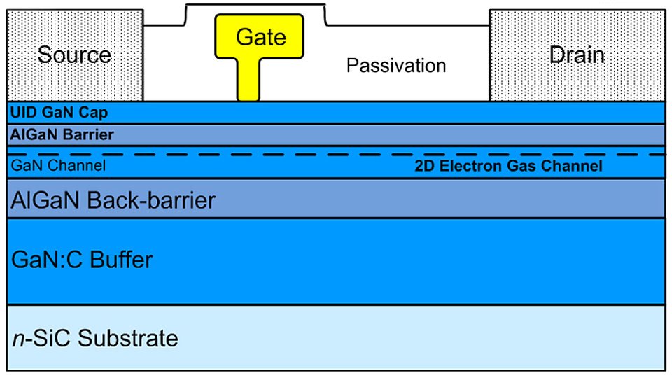
The FBH developed new GaN‑based heterostructures on conductive low‑cost substrates that unite enhanced vertical insulation for transistors with high off‑state blocking capability and low dynamic on‑state resistance. The GaN‑based epitaxial structure combines a GaN:C‑buffer for vertical insulation and high lateral breakdown strength, a low Al content AlGaN back‑barrier to separate the carbon doping from the UID GaN channel layer, and UID GaN cap encapsulation (see Fig. 1).
Switching transients of packaged test devices with grounded substrate have been taken with a special in‑house set‑up. Fig. 2 (a) shows the drain voltage transients for off-state biases from 20 V to 500 V with insignificant increase of the on‑state voltage drop. The on‑state and off‑state gate bias is +1 V and ‑5 V, respectively. The dynamic on‑state resistance may then be calculated from the on‑state current and drain bias. Ron_dyn increases up to a drain bias of 250 V but saturates for higher off‑state voltages. Fig. 2 (b) shows the transients of the drain current and of the drain voltage for a 500 V / 500 mA switching event. A very low dynamic on‑state resistance increase of Ron_dyn / Ron_st = 2.6 (absolute resistance Ron_dyn = 33.5 Ω · mm) was measured for these conditions.
FBH research: 18.3.2013

