3D simulations guide the design of multichannel GaN tri-gate transistors
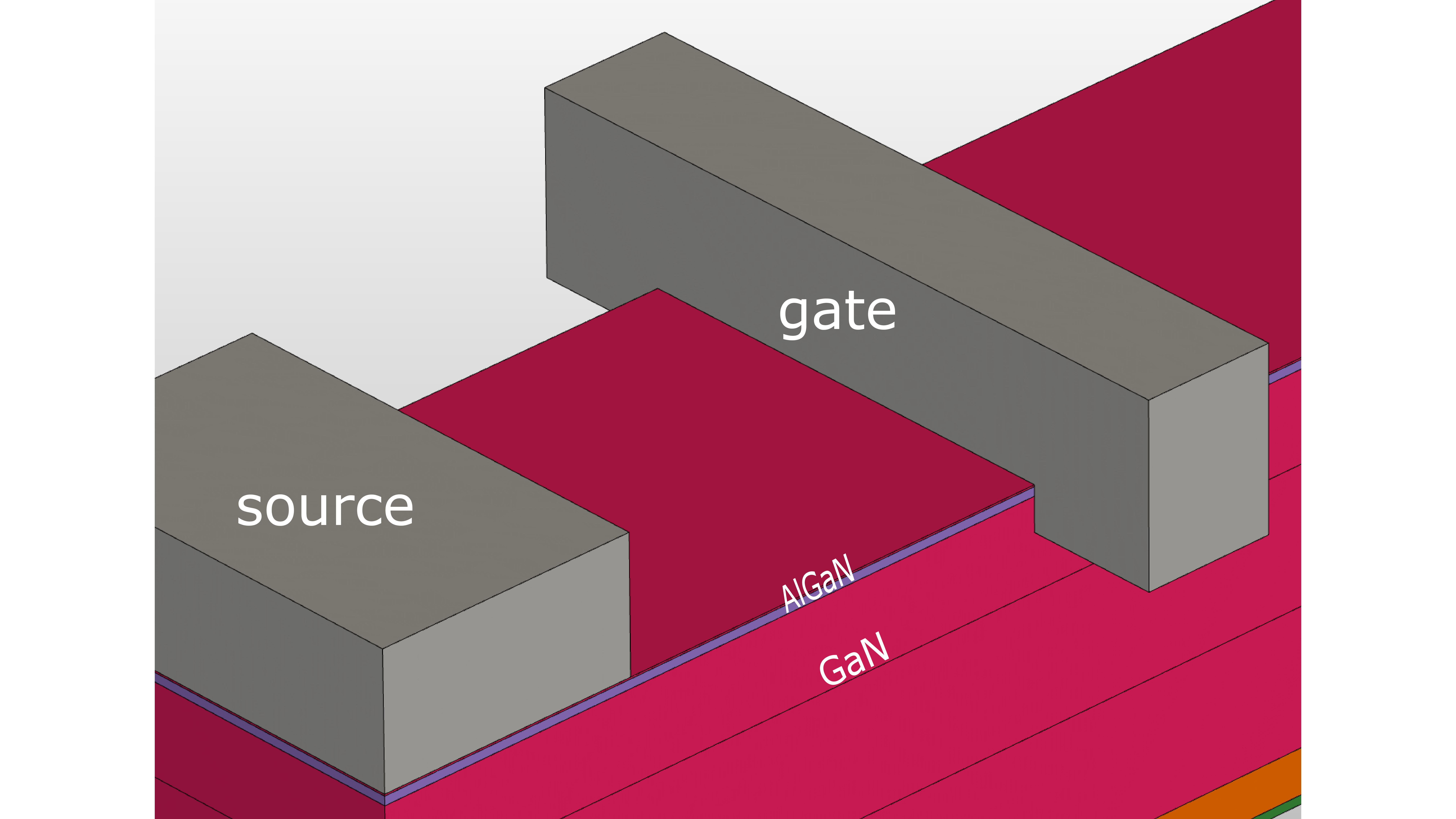
Fig. 1: TCAD tri-gate HEMT architecture.
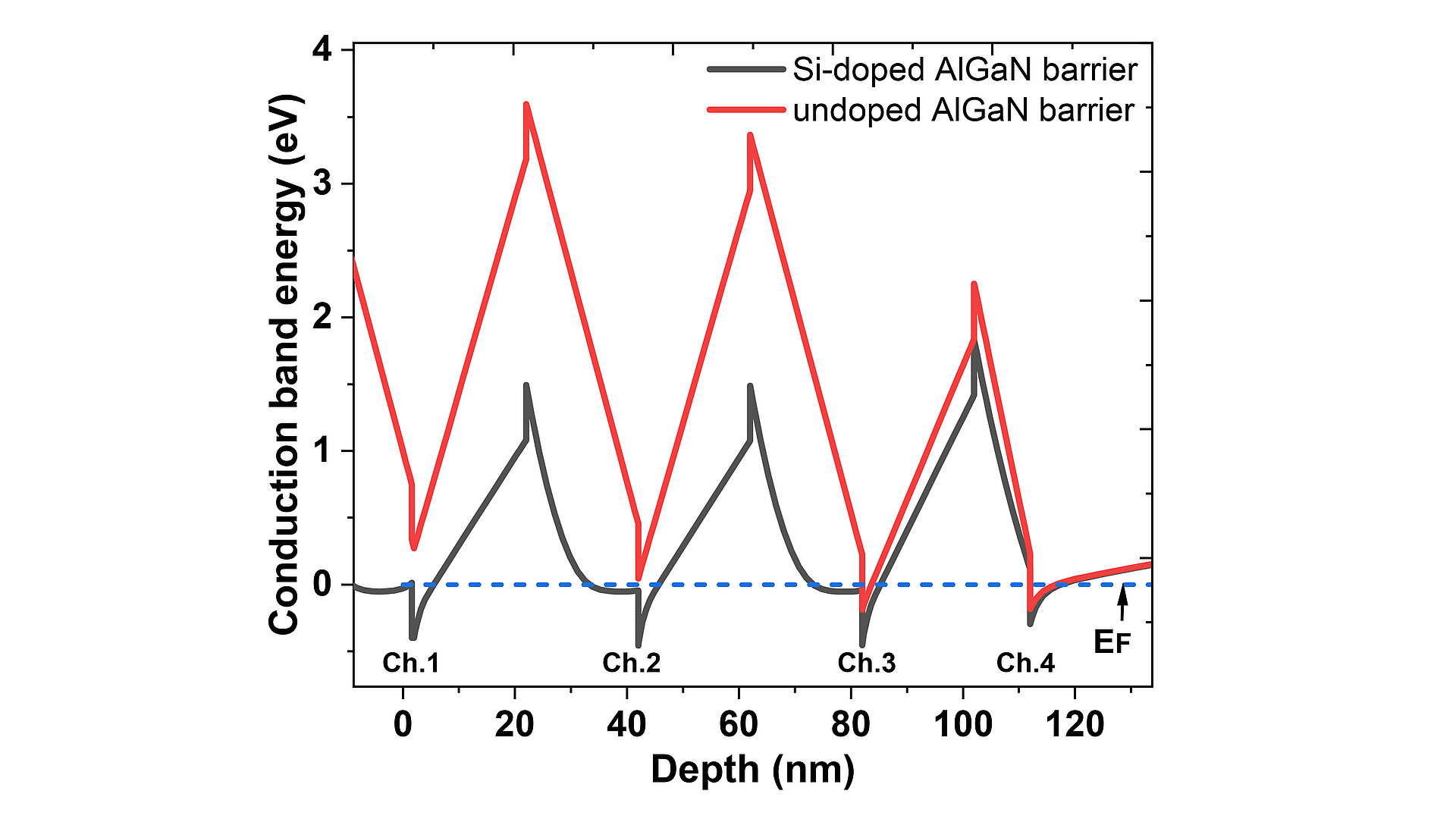
Fig. 2: Conduction band energy plots for two four-channel heterostructures, with and without selectively Si-doped AlGaN barriers.
Stacked channels could increase the current capacity of GaN transistors, but buried channels can become depleted. FBH's 3D simulations show how selective silicon doping helps populate the channels in a four-channel tri-gate design.
GaN is a key material for next-generation high-frequency and high-power electronics. Its high breakdown strength, high electron velocity and excellent thermal properties enable transistors to operate at high voltages, frequencies and power densities. Despite rapid progress, the performance of lateral GaN devices remains well below the theoretical capabilities of the material. Tri-gate GaN devices take the material advantages a step further by introducing three-dimensional control of the conducting channel.
In conventional planar AlGaN/GaN HEMTs, the current flows through a two-dimensional electron gas (2DEG) formed at the AlGaN/GaN interface. The gate controls this channel primarily from above. In a GaN tri-gate device, the gate controls the channel from both sides (Fig. 1). This tighter control could improve switching characteristics, reduce unwanted leakage and offer new possibilities for scaling and device design.
Even greater potential arises when the tri-gate concept is combined with multiple AlGaN/GaN channels. Several AlGaN/GaN heterostructures are stacked vertically, creating multiple conducting channels within the same device. Each channel contributes to the total current, increasing the available conducting cross-section and enabling higher current densities.
The challenge is to populate every channel while keeping sheet resistance low and the stack thin enough to fabricate. Barrier and channel thickness, as well as doping levels, all influence the result. Our 3D TCAD simulations show that very thin channels can lead to depletion of the 2DEG due to high electric fields at the channels. The conduction band energy plot, in this example on a four-channel heterostructure, demonstrates that n-type silicon doping of the barrier is essential to form the 2DEG in the buried channels and thus enable the successful implementation of multi-channel tri-gates (Fig. 2).
Multi-channel AlGaN/GaN tri-gate devices could therefore combine the material advantages of GaN with two complementary concepts: more channels for higher current capability and three-dimensional gating for tighter channel control. The simulations provide guidance for designing these devices. Fabricated transistors and measurements will be needed to establish whether the predicted benefits translate into better RF and power-device performance.