All-semiconductor PCSEL with novel unit cell design
High power edge-emitting lasers are widely used in material processing, fusion concepts and more applications due to their high conversion efficiency. However, they operate with low beam quality and the resulting low brightness prevents them from competing directly with established industrial lasers, such as fiber lasers. Photonic crystal surface emitting lasers (PCSELs) emit a high-power single-mode beam using a two-dimensional photonic crystal. Furthermore, they enable scaling of the optical output power by increasing the device size while maintaining a round single-mode beam.
Until recently, all high-power PCSEL utilized embedded air voids as the unit cell feature of the photonic crystal. In cooperation with Weierstrass Institute in Berlin, we have proposed an alternative all-semiconductor approach using a stretched isosceles triangle (SIT) as the unit cell feature (see Fig. 2a) [1, 2]. Simulations predict multiple 100 W of optical output power in a single-mode beam for a 2 mm device, demonstrating that the design is a promising approach for high-power PCSELs [3, 4].
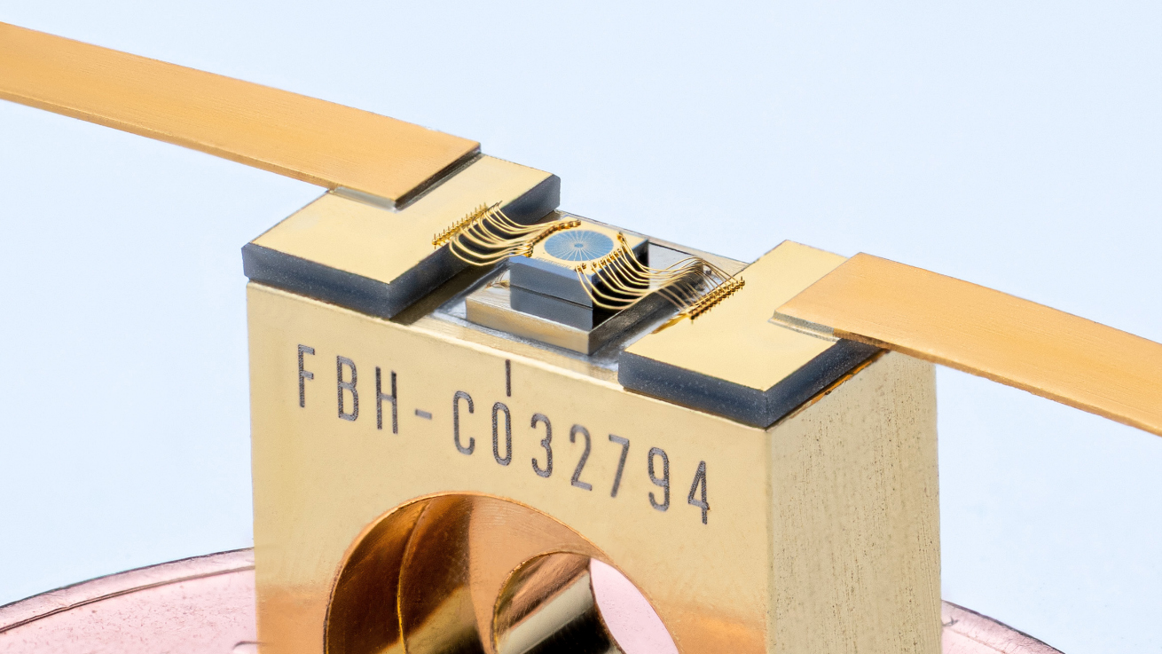
To realize our designs, we use a two-step metalorganic vapor phase epitaxy (MOVPE). After a first growth step, the triangles are etched out of a continuous InGaP layer using e-beam lithography and inductively coupled plasma reactive ion etching (ICP-RIE). In the second step, the free-standing triangles are overgrown and the rest of the structure is finished. An electrode with a circular emission window is established on the n-side to enable outcoupling of the beam [5]. The chips are then cleaved out of the wafer, mounted p-side down onto a c-mount and electrically contacted via bond wires for characterization.
We recently presented the first measurement results for the first generation of all-semiconductor PCSELS fabricated at FBH. The devices have a unit cell size of a ≈ 316 nm for an emission wavelength of λ ≈ 1070 nm. The measurements shown here were performed on a device with a photonic crystal size of 700 µm and a p-contact size of 650 µm. The pulsed power-current-voltage characteristics are shown in Fig. 1a. Lasing behavior can be seen with output powers of above 2.5 W, the highest yet reported from an all-semiconductor PCSEL at wavelengths around 1 µm. To bypass thermal effects, we performed measurements under pulsed condition using a pulse width of 500 ns. The optical power loss due to absorption in the 400 µm thick substrate layer is estimated to be roughly 50 % of the output power at the photonic crystal. Due to non-optimal processing, the unit cells have an asymmetry along the x = y diagonal, which leads to a change in the mode selection and suppression of higher order modes. This results in elongated far fields along one of the crystalline axes (Fig.1b).
Fig. 2a shows the unit cell design, while Fig. 2b presents a slice reconstruction of the unit cell taken from a special angled lamella using scanning transmission electron microscopy (STEM). This reconstruction confirms that the unit cells are smaller than designed and exhibit the observed asymmetry along the x = y diagonal. This is an explanation for the experimental findings and gives us important information for the further optimization on all-semiconductor PCSELs.
This work was performed in the frame of the project PCSELence (K487/2022) funded by the German Leibniz Association.
Publications
[1] B. King, H. Wenzel, E. Kuhn, M. Radziunas, P. Crump, “Design of very-large area photonic crystal surface emitting lasers with an all-semiconductor photonic crystal,” Opt. Express 32 (2024)
[2] “Großflächige oberflächenemittierende Hochleistungs-Einmoden-Vollhalbleiter-Photonischer-Kristall-Laser”, DE 10 2024 116 972 B4
[3] M. Radziunas, H. Wenzel, B. King, P. Crump, E. Kuhn, “Dynamical simulations of single-mode lasing in large-area all-semiconductor PCSELs,” Opt. Letters 50 (2025)
[4] L. Kuen, E. Kuhn, O. Senel, H. Wenzel, P. Crump, M. Radziunas, “Modeling and Simulations of Large-Area All-Semiconductor PCSELs,” IEEE Journal of Selected Topics in Quantum Electronics Vol. 32, No. 6 (2026)
[5] P. Sammeta, O. Senel, O. Brox, H. Wenzel, P. Della Casa, R.-S. Unger, C. Stölmacker, A. Knigge, P. Crump, “Demonstration of large area all-semiconductor photonic crystal surface emitting lasers,” Electronics Letters 62 (2026)