Towards Ka-band: 20 GHz large-signal performance of 150 nm gate GaN HEMTs
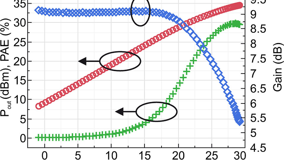
Fig. 2: Load-pull measurement results of 12 x 75 µm transistors (Vds = 28 V, Id = 30% Idss, tune for maximum Pout)
Ka-band GaN MMICs are gaining considerable interest for high data rate satellite links. In frame of the European FP7 project GaNSAT FBH develops K- and Ka-band MMICs for powering beam steering satellite transceivers. The project consortium jointly develops K-band amplifiers (about 20 GHz) for the satellite downlink and Ka-band low noise amplifiers (around 30 GHz) for the satellite borne receivers.
The recently introduced novel gateb process modules towards Ka-band GaN MMIC fabrication have now been combined with epitaxial structures well-adjusted to short gate lengths of 100 nm or 150 nm. They result in an improved electron confinement to the channel and high output power density. The improved epitaxial design is suitable for transistors with gate lengths down to 100 nm.
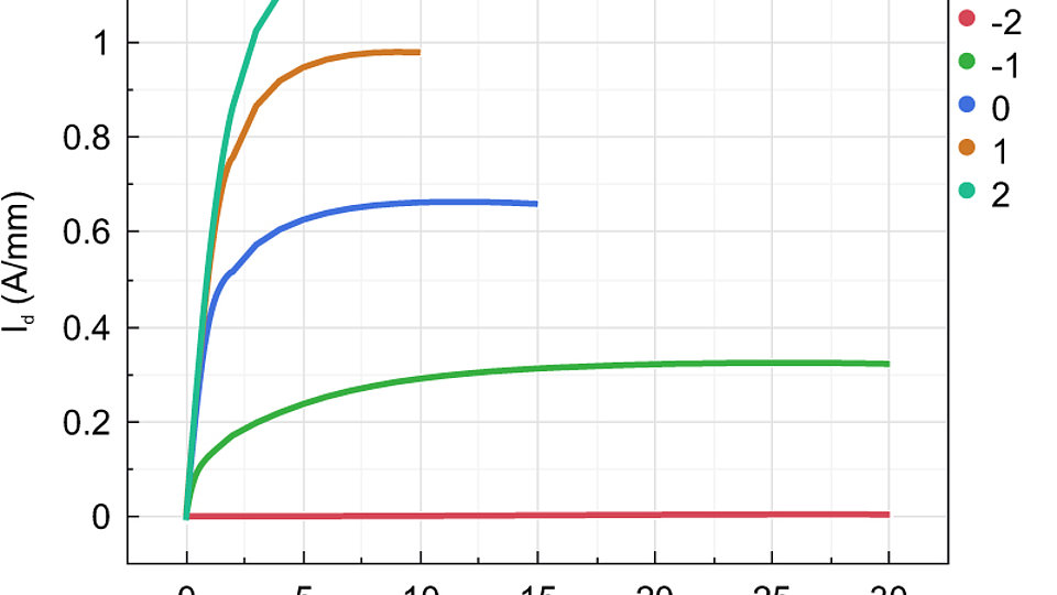
According to Fig. 1 the DC output characteristics of devices with 150 nm gate length show a maximum drain current density of Ids_max ~ 1.2 A/mm – a very competitive value ensuring high specific microwave power levels. The transistors pinch off at a gate voltage of -2 V and do not show any punch-through effect up to Vds = 30 V. In order to optimize the fundamental cells for a 10 W K-band power amplifier a design study comprising scaled transistors with different gate finger lengths and finger counts per transistor cell has been undertaken. An important selection criterion is the question to which degree the power gain of the devices degrade when they are scaling in finger count and gate width. In this connection, transistors with 75 µm unit gate width show almost no decrease in gain while increasing the number of fingers from 2 to 16. All these pre-selections were based on pulse S-parameter measurements at different bias points.
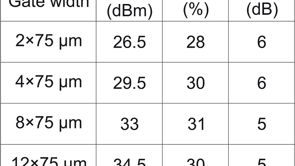
In order to determine the large-signal RF behavior of the devices, load-pull measurements of transistors with different gate configurations were performed at a drain bias of 28 V. Results of these measurements are summarized in table 1. The devices allow for a microwave output power density more than 3 W/mm and a power added efficiency (PAE) of about 30% at 20 GHz. The power gain at saturated output power is in the range of 6 dB. All these data correspond to the current state-of-art. Power cells comprising of 12 x 75 µm geometry have been finally selected to build the fundamental cells of the current 10 W K-band amplifier designs. Fig. 2 depicts 20 GHz load-pull measurements of the selected cells. They deliver a saturated out power of 3 W, a linear gain of 9 dB, and a PAE of 30%.
Publication:
K. Y. Osipov, S. A. Chevtchenko, O. Bengtsson, P. Kurpas, F. Brunner, N. Kemf, J. Würfl, G. Tränkle, "Current Dispersion in Short Channel AlGaN/GaN HEMTs", Int. Conf. on Compound Semiconductor Manufacturing Technology (CS ManTech 2015), Scottsdale, USA, May 18-21, pp. 269-272 (2015).


