Reduced dislocation density – patterning of sapphire to fabricate templates for GaN/AlGaN epitaxy
UV light emitting diodes (LED) are highly attractive for various applications and have the potential to replace, for example, mercury vapor lamps for UV water purification and UV curing of polymers. Accordingly, the epitaxial growth of GaN/AlGaN for light emitters in the ultraviolet (UV) spectral range has increasingly attracted interest in recent years. To improve the internal quantum efficiency of such LEDs, epitaxial layers with reduced dislocation densities are required. Epitaxial lateral overgrowth (ELO) on patterned sapphire substrates can help to reduce strain and dislocation density in GaN/AlGaN layers.
Studying such effects requires a number of suitable pseudo substrates (templates) with different pattern designs. At FBH, these templates are fabricated by applying photolithography and plasma etch processes. The patterned templates are processed on bare sapphire substrates. Sapphire (Al2O3) belongs to the hardest materials in semiconductor technology. It is resistant and extremely difficult to etch chemically, which makes patterning very challenging. Because of properties like high aspect ratio imaging, vertical side-wall angle, and excellent dry-etch resistance, KMPR photoresist has been used as etch mask combined with a SiNx sacrificial layer. Honeycomb-like patterns in KMPR were fabricated by i-line stepper lithography.
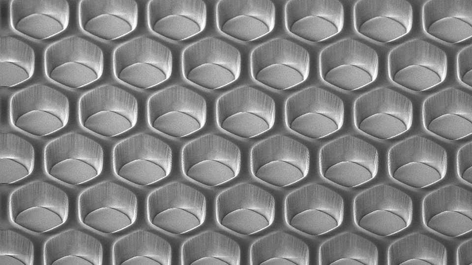
Reactive ion etching is the process of choice to transfer such patterns with sufficient depth into sapphire substrates. Due to the high lattice energy of sapphire high ion energies and ion densities are needed. An etching process with inductively coupled plasma (ICP) combines both requirements and is proven to be the best method for such patterning. Chlorine-containing gases can be used as etch gases for Al2O3 because volatile chlorides are formed. For etching metal oxides, such as Al2O3, it has been found that an excess of BCl3 in a BCl3/Cl2 mixture facilitates relatively high etching rates. Because of the limited thermal stability of the KMPR photoresist, the temperature of the wafer needs to be controlled during etching. Hence, the back side of the sapphire substrate is directly cooled with helium during plasma processing. Due to the limited layer thickness of KMPR, optimum etch conditions have been developed that ensure a sufficient etch selectivity between the KMPR etching mask and the Al2O3. With the etch recipes developed at FBH honeycomb-like patterns featuring a depth above 4 µm have been fabricated. As Fig. 1 shows, the etched surface is very smooth and free of residues. After wet-chemically removing the etch masks consisting of KMPR and SiNx the final structures are now ready for epitaxial lateral overgrowth.
Publication:
S. Hagedorn, E. Richter, U. Zeimer, D. Prasai, W. John, M. Weyers, "HVPE of AlxGa1-xN layers on planar and trench patterned sapphire", J. Cryst. Growth, vol. 353, no. 1, pp. 129-133 (2012).
FBH research: 08.04.2014
