New Focused Ion Beam System for Device Characterization and Rapid Prototyping
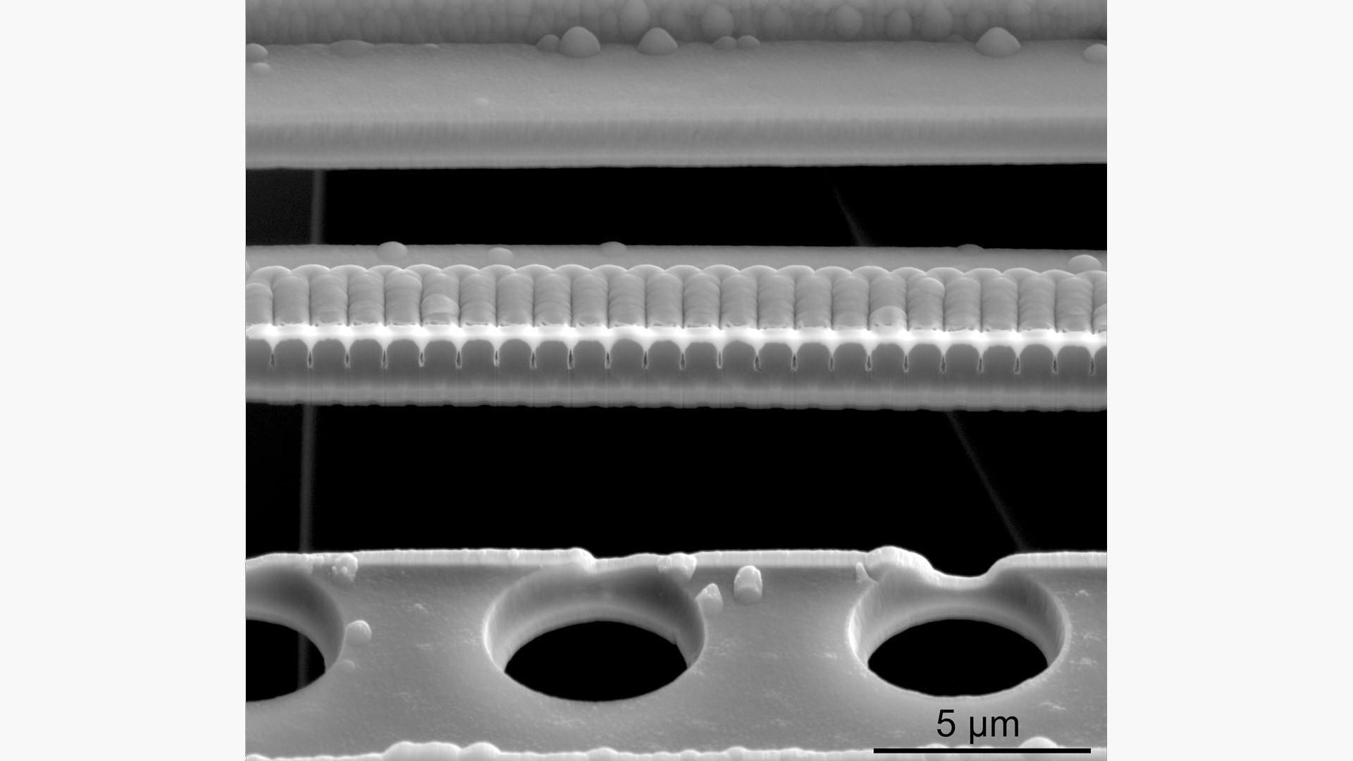
Fig. 1: SEM micrograph showing a cross-sectional FIB cut in a silicon oxide-based waveguide.
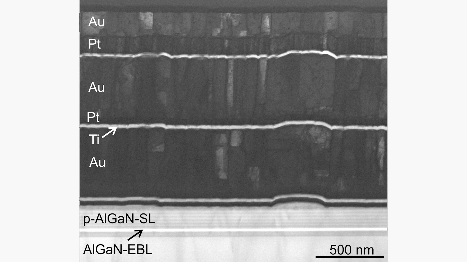
Fig. 2: Bright-Field SEM image acquired in transmission of a FIB lamella showing metal contact layers and an upper part of an AlGaN-based LED operating in the ultraviolet wavelength range.
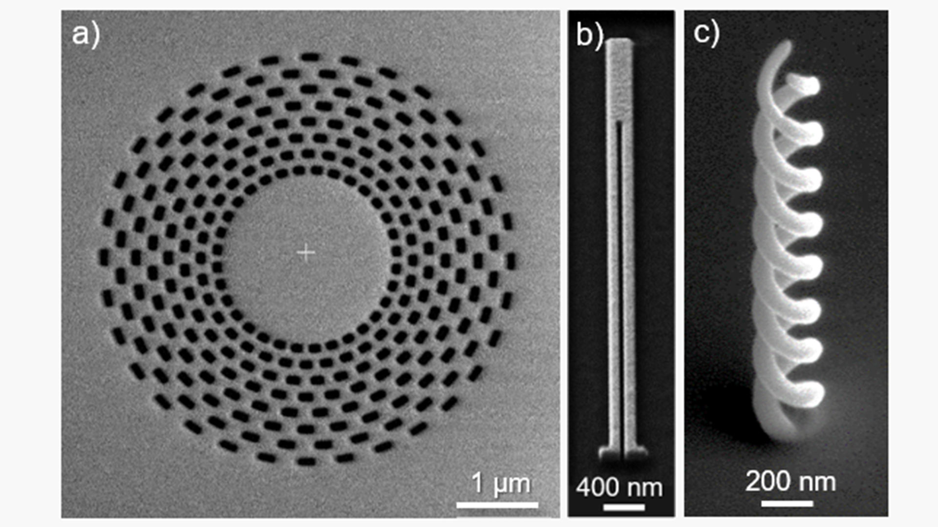
Fig. 3: a) Photonic bull’s eye cavity in suspended SiN, b) plasmonic two-wire waveguide and c) double helical antenna, both from gold.
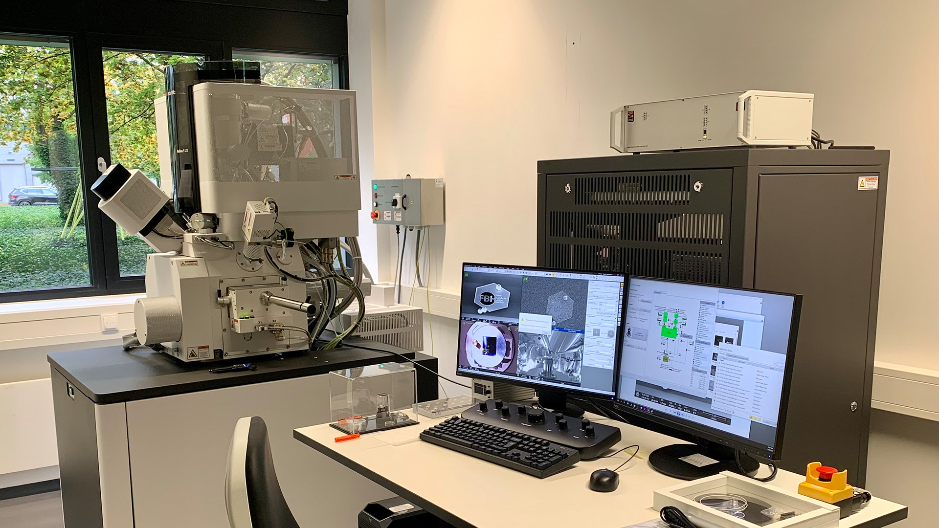
Fig. 4: Helios 5 UX dual beam system at FBH.
Beams of charged particles such as ions and electrons can be used for high-resolution imaging of materials and devices but also for direct material modification on the nanoscale. The impact of ions can remove material locally in a maskless process by physical sputtering. The choice of ion species determines the most appropriate use cases in materials and device analysis but also for rapid prototyping of nanophotonic components
The newly installed Thermo Fisher Helios 5 UX dual beam system combines a focused ion beam (FIB) column with a scanning electron microscopy (SEM) column. This allows top-down and bottom-up processes based on gallium ions or electrons to be performed in one instrument. In addition, SEM imaging allows in situ control of the manufacturing process. Add-ons available include various types of detectors, injection systems for local precursor gas delivery, a nanomanipulator with rotation capability for lift-out and pick-and-place assembly, plus heating and cooling tables.
Material investigations and failure analysis of devices
The focused ion beam can be used to prepare spatially localized cross-sections of devices for direct visual examination with the SEM, as in the case of the silicon-oxide-based waveguide displayed in Fig. 1. This provides valuable information, allowing further improvement of design, fabrication processes as well as device performance. FIB-based failure analysis is currently being performed for LEDs, fin field-effect transistors, and for various material platforms as a part of device processing optimization.
Additionally, electron-transparent lamellae are prepared at specific locations of the devices to be examined later by transmission electron microscopy (TEM). Fig. 2 shows such a lamella of an AlGaN-based LED directly after preparation. TEM analysis allows for microscopic investigation of epitaxially grown layer sequences on the nanometer scale concerning their crystalline structure, compositional homogeneity and crystal defect distribution. It therefore plays a crucial role in correlating material properties with device characteristics and allows targeted tuning of fabrication and processing parameters. At FBH, the following topics are currently being investigated using TEM: structural quality of facet coatings in AlGaAs-based laser diodes, optimization of n- and p-type contacts on group-III nitride-based laser, and light emitting diodes.
Prototyping of cavities, waveguides and antennas
Another important application involves ion beam patterning for the fabrication of two-dimensional geometries with structural features smaller than 20 nm. As a complementary technique to lithographic fabrication, it can be successfully used for the fabrication and local modification of on-chip resonators, waveguides and antennas in a rapid prototyping approach. This includes patterning cavities of photonic crystals or Bragg mirrors in nanofibers of glass or in floating dielectric membranes. In a collaborative effort with the "Photonics in 2D Materials" group at FSU Jena the bull's eye resonator shown in Fig. 3a) was realized by using this technique. In the same way, nano-optical components can be engraved directly on the chip, such as the plasmonic waveguide made of single-crystal gold shown in Fig. 3b).
The full potential of nanofabrication in the dual-beam instrument can be realized when both of the focused particle beams are used for structural modifications. The electron beam can write nanostructures directly by local dissociation of precursor molecules, similar to 3D printing but without a resist. In this way, truly three-dimensional nanostructures, such as the double helix antenna shown in Fig. 3c), can be fabricated directly at specific target positions on the chip. Combined with ion beam-based patterning, complex devices can thus be fabricated in a single instrument.
This work was supported by the EFRE – European Fonds for Regional Development under grant number 1.8/17. Furthermore, we would like to highlight our lead participation in the EU Cost Action CA 19140 ‘FIT4NANO – creating a research and innovation environment to further develop focused ion technologies for nanomaterials, https://www.fit4nano.eu.