New electro-thermal model for GaN-HEMT power transistor description
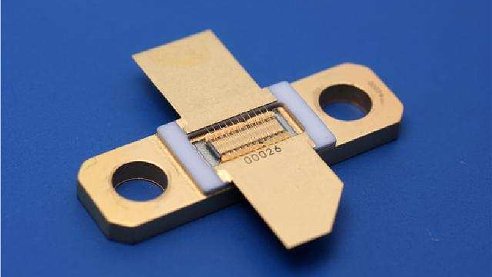
The development of GaN microwave power transistors is one focus area of the FBH. Such transistors consist of several cells, comprising several fingers each, and are soldered in a package (Fig. 1). Therefore, the power bars are relatively large and complex structures. The question to what degree the single cells are operated in-phase and the power distribution is homogeneous over the cells is decisive for the available output power and efficiency. In order to analyze and understand the interaction of the power bar’s parts, we developed a distributed electro-thermal network model for our power transistors.
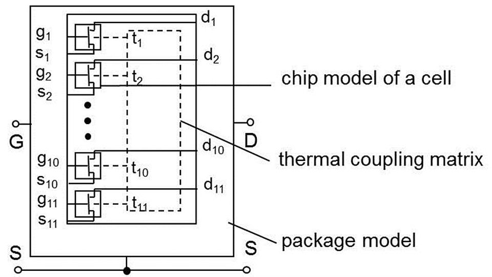
The bar model consists of a package model, a network describing the thermal properties and coupling of the cells, and the chip models of the power cells (Fig. 2). The package model is based on electro-magnetic simulations, while the thermal model is derived from FEM (finite elements method) calculations of the power bar structure. Each cell of the power bar is represented by a non-linear large-signal transistor model. This combination of transistor description, package model, and the full thermal representation including coupling between the transistor cells is a novel approach.
The comprehensive model allows DC and radio-frequency analysis. For example, RF power and power loss distributions as well as the temperature distribution within the bar can be obtained. This way, the interconnections of the cells can be optimized. The determination of instabilities within the power transistor is another application of the newly developed model. Conventional models used so far are not appropriate for that purpose.
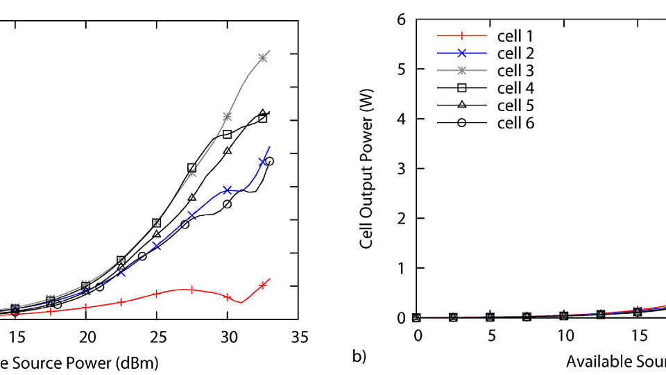
As an example, Fig. 3 shows the RF output power of the individual cells with increasing total RF input power of the bar. Cell 1 is located at the end of the bar, cell 6 in the middle (see Figs. 1 and 2). If the cells are connected in the standard way, the cells of the power bar deliver very different output powers (see Fig. 3a). Internal oscillations between the cells drastically reduce the overall gain of the bar. Introducing ohmic resistances between the cells the oscillations between the cells are suppressed and the power is distributed now much more evenly (Fig. 3b). As a result, total output power and efficiency of the bar almost double.
Publication:
F. Schnieder, O. Bengtsson, F.-J. Schmückle, M. Rudolph, and W. Heinrich, "Simulation of RF power distribution in a packaged GaN power transistor using an electro-thermal large-signal description", accepted for publication in IEEE Transactions on Microwave Theory and Techniques, 2013.
FBH research: 29.05.2013


