New ALD-etch cluster tool promotes FBH’s device technology
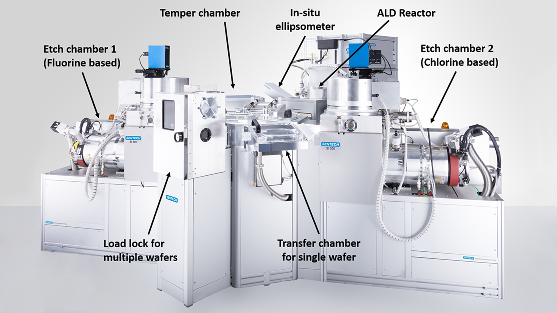
Fig. 1: Setup of the ALD-etch cluster tool at FBH.
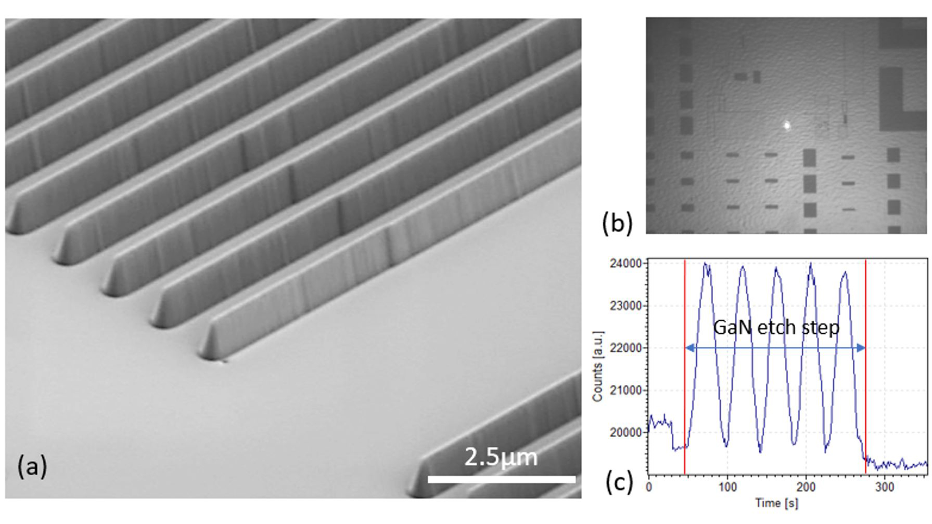
Fig. 2: (a) SEM image of a FinFET pattern etched into the GaN surface using a SiNx hard mask. (b) Camera view of the surface showing the bright laser spot for in-situ interferometry. (c) The recorded laser intensity during etching for etch depth control.
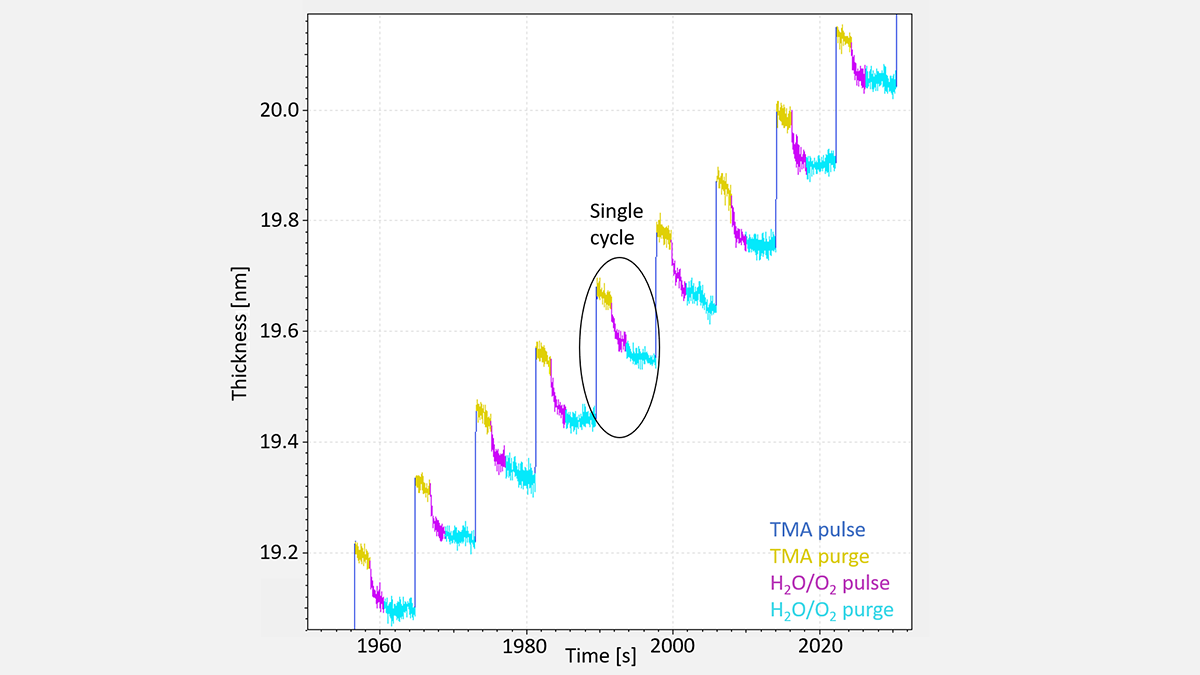
Fig. 3: In situ ellipsometry data taken during an atomic layer deposition. The different colors indicate the 4 steps for one deposition cycle of Al2O3.
For the development of novel device concepts like lateral metal-insulator semiconductor field-effect transistor (MISFETs) and vertical GaN-transistors, we have put a new 4-chamber cluster tool manufactured by SENTECH into operation. It allows to run atomic layer deposition (ALD) and inductively coupled plasma (ICP) etch processes consecutively without breaking the vacuum conditions. This unique concept of etch and deposition methods in one tool offers well-defined surface conditions and a low level of cross-contamination, enabling a high degree of integration.
The ALD-etch cluster tool at FBH (see Fig. 1) consists of two ICP etch chambers, an annealing chamber, and an ALD reactor. All of them are connected by a central transfer module. There are two wafer load chambers, one for single wafer load and one for a batch processes cassette (up to 12 wafers). Each etch chamber is equipped with an SLI670 interferometer mounted on top of the ICP source.
The two etching systems enable ICP etching processes in successive steps with different etching chemistries. For example, fluorine-based chemistry can be used to perform hard mask opening and resist removal steps. Subsequently, GaN etching can be performed using chlorine-containing gases without removing the wafers from vacuum. As an example, Fig. 2a shows a tilted SEM image of a fin-gate structure precisely etched to 730 nm depth into the GaN epitaxial layer by chlorine-based process. The fin field-effect transistor (FinFET) pattern was pre-defined by a SiN hard mask that previously had been opened in the fluorine etch chamber. The progress of each etch process can be monitored by in situ interferometry. The etch depth is observed on a position on the GaN surface that is visible as bright laser spot in a camera view (see Fig. 2b). The recorded laser intensity shown in Fig. 2c was used to stop the process after 5 periods of etching, i.e., at 230 s etch time, to reach the target etch depth of 730 nm.
After plasma etching, the substrates may be transferred to the annealing chamber that is able to reach temperatures of up to 500 °C. Here, the wafers can be treated under N2 atmosphere at pressures ranging from 200 Pa to ambient.
The ALD reactor is able to run thermal activated processes of up to 400 °C, or alternatively, plasma enhanced processes. In both cases, the gaseous precursors undergo self-saturating reactions on the substrate surface, resulting in a well-defined atomic layer by layer growth. Since the interface between substrate and the grown ALD film determines the final device properties, suitable pre-treatments such as H2, NH3, N2, and Ar-based plasmas can be used prior to ALD depositions. As the plasma is ignited by a remote source, substrate damage effects are minimized. For now, the growth of Al2O3 has been optimized, with TMA (trimethylaluminum) and H2O or O2 precursors. Qualification of these films for MISFET and FinFET devices is in progress. In parallel, experiments to grow HfO2 and SiNx have been started.
The growth of the films can be monitored in situ with an ellipsometer, where the typical single steps of the deposition cycles can be observed as shown in Fig. 3. This feature helps to control and to optimize the deposition process. Due to the self-limiting growth behavior, ALD films are known for their good conformality and uniformity. We could demonstrate a uniformity up to 99.6%.
With the new possibilities to etch, anneal and deposit in one single cluster tool, FBH will explore new opportunities for integrated device concepts.