Nanofabrication of suspended photonic crystal cavities in diamond
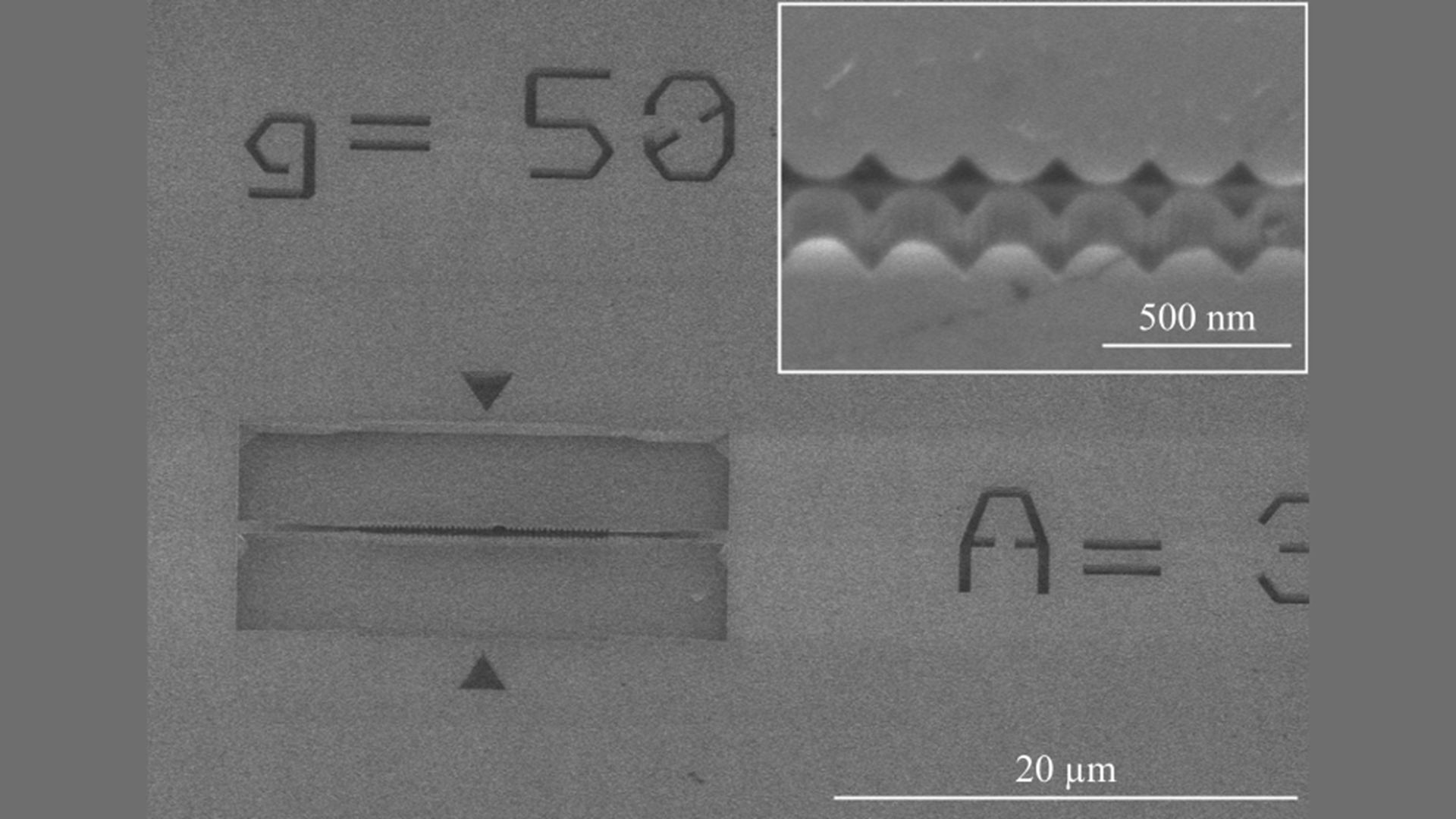
Fig. 1: SEM showing a 30° tilted view of a suspended cavity. The nanostructure is about 20 µm long and 275 nm thick. Inset: closed-up view of one cavity, showing the periodic modulation of its width.
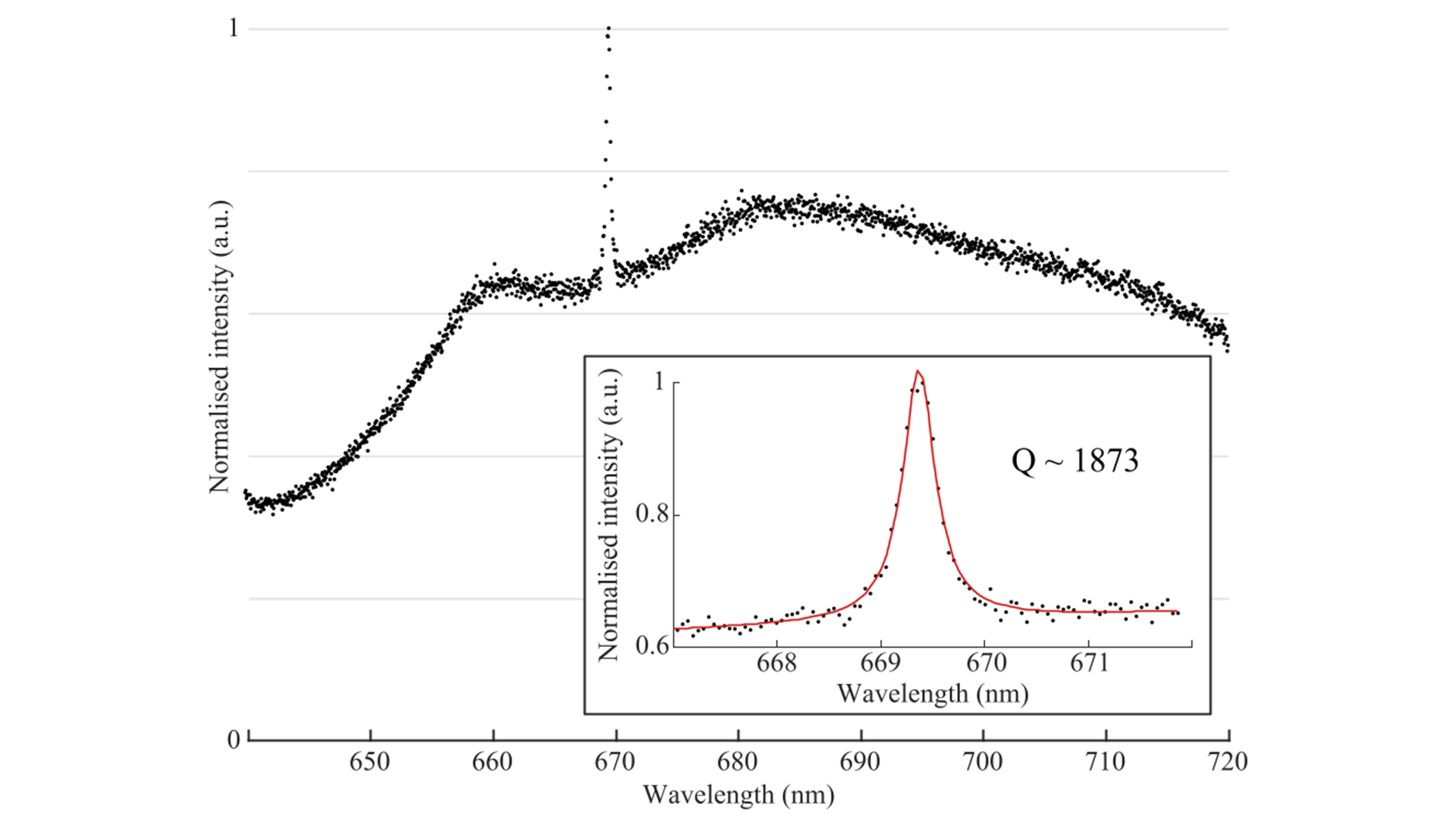
Fig. 2: Fluorescence spectrum collected from one of the fabricated cavities at room temperature. The sharp peak that sits on top of the broad background emission corresponds to the resonance frequency of the cavity mode. The inset shows a zoom into the spectral range of the cavity mode. From a Lorentzian fit of the data (red line), we evaluated a Q-factor of about 1873.
Photonic crystal cavities have been used to study the interaction of light with matter already for some time. Nowadays, they become more and more important devices for the development of quantum communication technologies. Formed by a periodic modulation of the refractive index of a dielectric material, these devices can be engineered to confine light of specific wavelengths, that is the resonance wavelength of the cavity. When an optical quantum system, such as a color center in diamond, is placed inside the cavity, its coupling with the electromagnetic field is increased. The enhancement of the light-matter interaction that takes place in a photonic crystal cavity can be exploited to build quantum networks, for example. Such an interface ensures that information is efficiently transferred between a flying qubit (i.e. a photon) and a stationary qubit (i.e. the quantum system).
In our Joint Lab Diamond Nanophotonics we have now successfully fabricated suspended nanostructures in diamond by implementing a quasi-isotropic dry etching process in O2-plasma. The scanning electron micrograph (SEM) in Fig. 1 shows an example of such a device, which is about 20 µm long and 275 nm thick. In the inset, a close-up SEM shows the periodic modulation of the width of the nanostructure, which forms the optical trapping potential in this device. These photonic crystal cavities require full suspension from the substrate in order to trap light inside. However, this task was very challenging as diamond cannot be grown single crystalline in thin films of several hundred nanometers.
The devices were characterized in the optical laboratories at Humboldt-Universität zu Berlin, where emission spectra from the fabricated devices have been collected at room and cryogenic temperatures. An example of such a spectrum is shown in Fig. 2, where the sharp peak – the resonance – of the cavity mode is visible on top of the broad emission from the phonon side band of the nitrogen-vacancy defect centers present in the diamond matrix. By fitting all the collected peaks with a Lorentzian function, the quality factors of the fabricated cavities could be evaluated. Values as high as 2400 were found.
The new design of the presented photonic crystal cavities was originally proposed by our partners in the research group Integrated Quantum Photonics at HU Berlin. FBH will further develop and optimize the fabrication techniques to enable a reliable production of suspended photonics crystal cavities with high quality factor.
The discussed results were realized within the projects “Diamant-Nanophotonik für On-Chip Quantentechnologien” (DiNOQuant, project number 13N14921), Photonisch-Integrierter Quantencomputer (QPIC-1, 13N15858), “Quanten-Photonisch Integrierter Skalierbarer Speicher” (QPIS, 16KISQ032K) supported by the Federal Ministry of Education and Research of Germany (BMBF).