InP transistors with improved thermal resistance due to integrated diamond heatsink
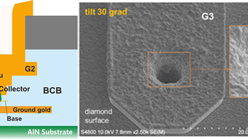
Fig. 1: Schematic cross section of diamond layer integration into the InP DHBT process (l.), SEM image of metal-filled via-hole (r.)
In the last years, the interest in applications operating in the mm-wave to sub-THz frequency range has steadily increased. Thus, InP double hetero bipolar transistors (DHBTs) are popular in analog and digital mm- and sub-mm-wave circuits, delivering high RF output power and high speed. This is due to the unique material properties of the compound semiconductor indium phosphide (InP), which allow for fast electron transport and provide high breakdown voltage. An important boundary of device operation lies in the HBT’s thermal resistance Rth which not only limits the RF output power of the device, but also reduces the small signal gain through self-heating of the device.
In FBH’s transferred substrate process, the HBT’s active semiconductor layer stack is bonded to a ceramic aluminum nitride (AlN) host wafer, featuring a thermal conductivity of more than 170 W∙m-1∙K-1. The wafer bonding process uses benzocyclobutene (BCB) as an adhesive between the active layers and the AlN host substrate. BCB, a polymer, exhibits only a low thermal conductivity of 0.29 W∙m-1∙K-1 and therefore may impede the heat flow, even if the thickness of the bonding layer is less than 5 µm. To improve heat sinking of the HBT, within the VIP project AVTE a 10 µm thick nanocrystalline chemical vapor deposition diamond (NCD) layer with a thermal conductivity of 600 - 800 W∙m-1∙K-1 is added on top of the collector microstrip wiring. Exhibiting very low dielectric losses, the diamond layer can be brought into direct contact with the collector wiring without incurring additional RF losses (see Fig. 1). The NCD layer efficiently transports the generated heat away from the device, acting as a heat spreader. From the NCD layer itself, the heat flows through large-diameter thermal vias towards the AlN host wafer which, in turn, is mounted on a heat-sink package surface.
The diamond layer is available on a Si carrier wafer. It is attached to the processed wafer surface in a second wafer bonding step at the end of the InP HBT fabrication process, using BCB. Then, the diamond’s silicon carrier wafer is removed in a combined mechanical and chemical process. Via holes through the diamond layer and the BCB bonding layer are dry-etched, exposing the collector wiring level G2. A thick electroplated gold layer (G3) makes an electrical and thermal connection to the top of the composite stack, providing the thermal heat sinking path for the device and serving as the contact pad metallization.
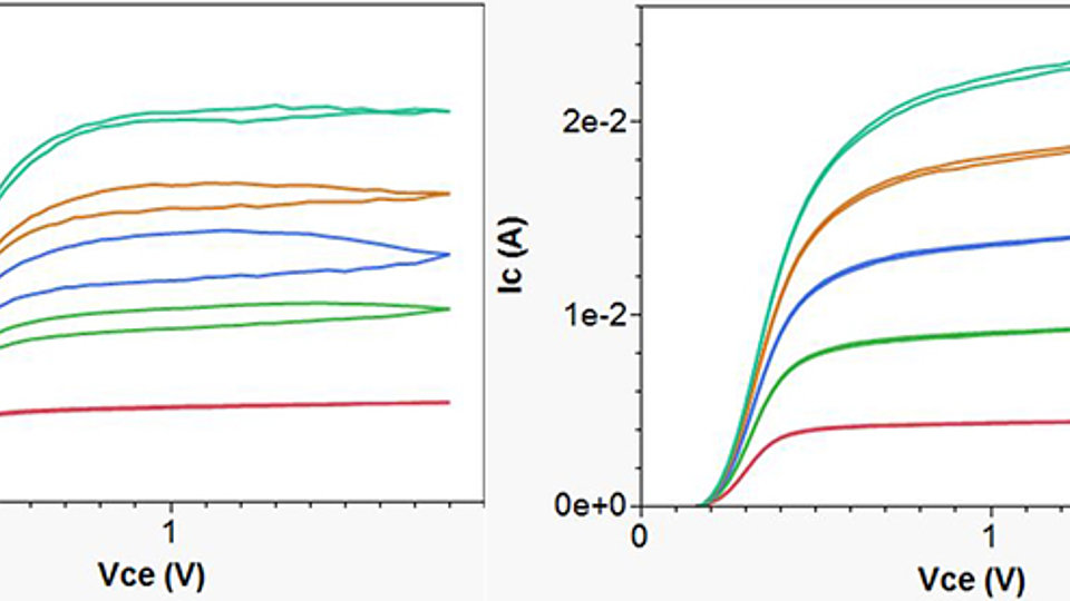
InP DHBTs were characterized by DC and RF measurements on the same wafer before and after diamond layer integration. A significant reduction of the hysteresis in DC output curves caused by self-heating could be observed with the diamond heat sink (see Fig. 2).
RF characterization showed no significant reduction in performance. The average current gain cutoff frequency fT, 358 GHz before and 321 GHz after diamond integration and the average maximum oscillation frequency fmax, 329 GHz before and 321 GHz after diamond layer bonding are within the measurement accuracy. First extraction of Rth with a DC method using the HBT's base-emitter junction as a thermometer before and after diamond heat sinking indicates a reduction in Rth of at least a factor of two (from 3 K/mW down to 1.3 K/mW), as had been predicted in thermal simulations.
Publication:
K. Nosaeva, W. John, N. Weimann, O. Krüger, and T. Krämer, "Development of a Via Etch Process through Diamond and BCB for an Advanced Transferred-Substrate InP HBT Process," presented at the 37th Workshop on Compound Semiconductor Devices and Integrated Circuits (WOCSDICE), Warnemünde, Germany, 2013, pp. 23–24.
FBH research: 22.10.2014

