Improved thermal management of InP high-power transistors
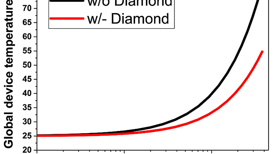
Fig. 2:TCAD simulation indicating the effect of adding a diamond heat sink on the global device temperature
Indium phosphide HBT technology is an ideal candidate for microwave applications in the terahertz range. Heterojunction bipolar transistors (HBTs) that are processed with the transfer substrate method have succeeded in suppressing significant parasitic elements responsible for lowering the device transit and maximum frequencies. However, a major drawback of transistors based on this technology is their thermal management. This gives heat sinking and heat spreading the utmost importance when designing such technologies for high power densities.
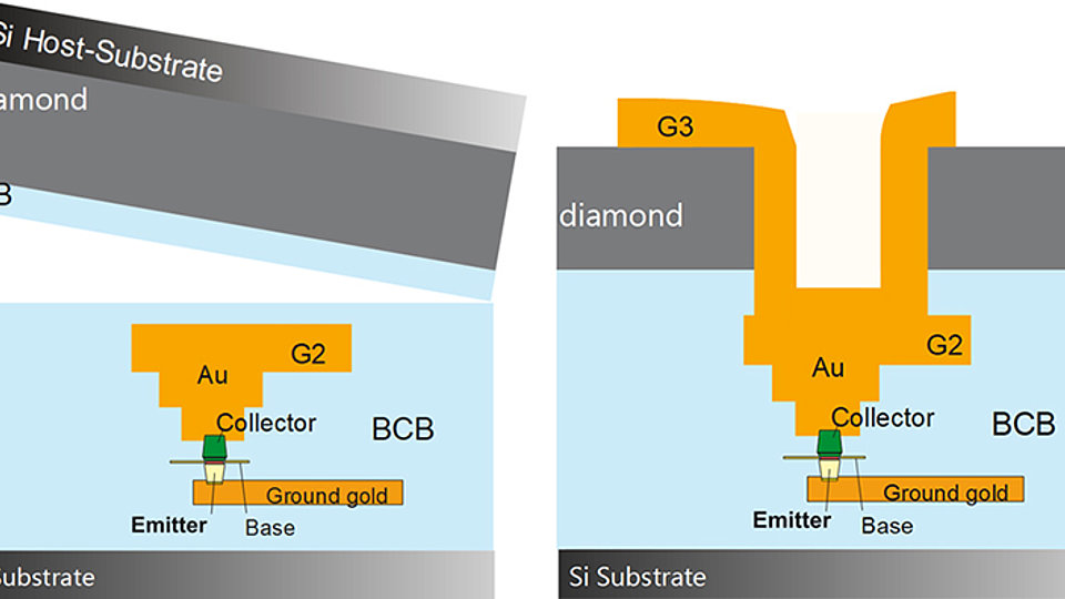
An in-house diamond wafer bonding process was used to enhance the thermal management of the wafer. The process relies upon a benzocyclobutene (BCB) bonding process in which a diamond layer grown by chemical vapor deposition on silicon is bonded on the existing InP/Si wafer as depicted in Fig. 1. Heat spreading takes place vertically through the collector, the G2 layer and then laterally through the diamond layer. Technology computer-aided design (TCAD) simulation shows the effect of the added diamond layer on the global transistor temperature as depicted in Fig. 2. At lower current values self-heating of the device is barely noticeable, and therefore the effect of the diamond is insignificant. At higher current densities the simulation predicts a decrease of approximately 20° C in the device temperature.
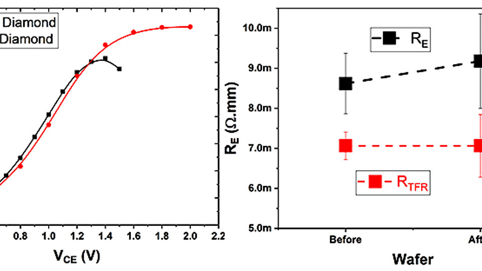
Thermal effects have a significant influence on the electrical properties of the transistors as seen from the suppression of the “kirk” effect in ft and the fmax values. To monitor the effect of the diamond boding module on the overall process stability, process control monitoring structures were measured before and afterdiamond bonding. Variation in the device contact resistance and the thin film resistor are seen to be negligible, indicating process stability and uniformity as seen from Fig. 3.


