Improved AlGaN UV photodetectors by interface conduction
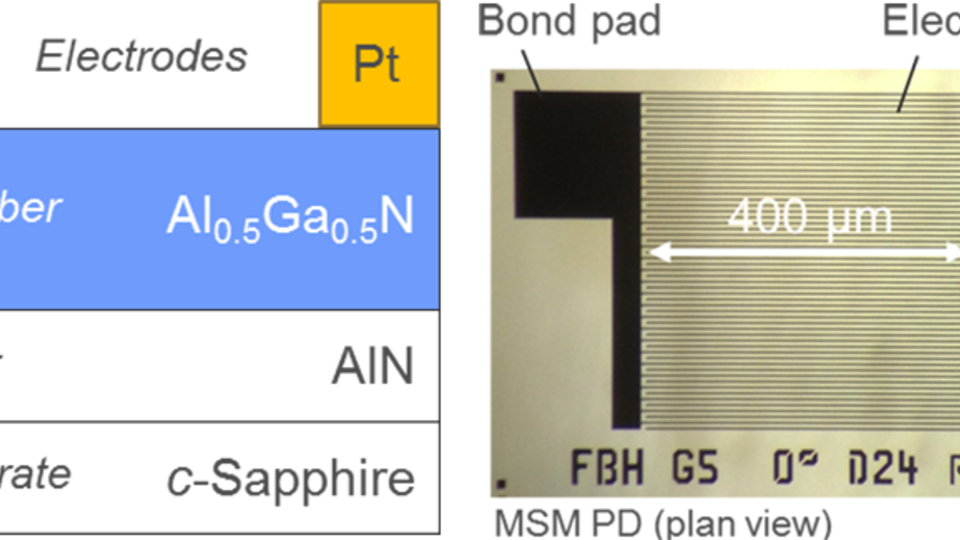
Fig. 1. Design of AlGaN/AlN MSM PD. Left: epitaxial layer stack (cross section). Right: electrode geometry (top view; yellow: Al0.5Ga0.5N, black: metal)
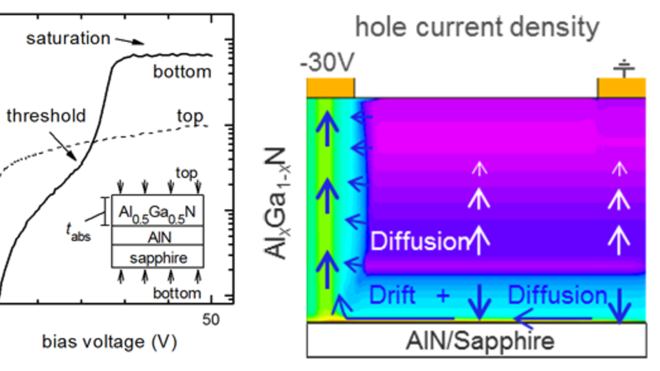
Fig. 2. Left: measured EQE characteristics of Al0.5Ga0.5N/AlN MSM PD of different absorber thicknesses tabs for top-side (FS) and substrate-side (RS) illumination. Right: simulated hole current density in the 0.5 µm thick AlGaN absorber for substrate-side illumination in saturation mode (-30 V)— see Ref. [1]
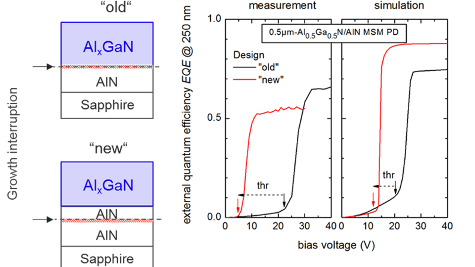
Fig. 3. Left: sketch of “old“ and “new“ layer design; arrows indicate growth interruption. Right: measured (left) and simulated (right) EQE characteristics of 0.5 µm thick Al0.5Ga0.5N/AlN MSM PD having “old” (black) or “new” (red) layer design — arrows indicate corresponding threshold positions.
The AlxGa1-xN material system is attractive for the detection of ultraviolet (UV) radiation. Owing to the dependence of the large band gap energy on Al mole fraction x (3.4 eV to 6.2 eV), the cut-off wavelength of photodetectors is adjustable between 365 nm and 210 nm. Moreover, the material is robust against UV-radiation. Due to their simple design (Figs. 1a and b) metal-semiconductor-metal photodetectors (MSM PD) require little effort in epitaxy and processing since no doping or ohmic contacts are needed.
We developed MSM PD with thin AlGaN absorber layers on AlN/Sapphire templates that show high external quantum efficiencies (EQE) saturating at about 70% when the PD is illuminated from the substrate side [1]. However, these high EQE values require a certain bias-threshold Uthr. According to 2D-simulations (ATLAS, Silvaco [2]), the observed threshold and saturation of the EQE (Fig. 2a) was explained by an efficient separation of photo-generated electrons and holes within the polarization field at the AlGaN/AlN heterojunction (Fig. 2b), making this a region of paramount interest for photodetection by AlGaN-based MSM PDs.
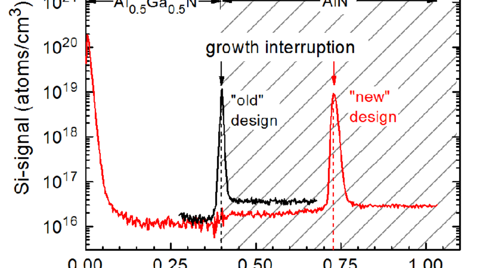
The AlN buffer layer is deposited by metalorganic vapor phase epitaxy (MOVPE) in a first growth run in a specially designed reactor for AlN growth. In the “old” design (Fig. 3a) the 0.5 µm thick AlGaN absorber layer is deposited subsequently in a second growth run, resulting in a bias-threshold of about 22 V (Fig. 3b). However, when an additional AlN interlayer is inserted before the AlGaN absorber (“new” design in Fig. 3a) the threshold voltage is reduced to a value of only 4 V. This is due to the donor Si, situated at the surface of the AlN buffer layer right before the second growth run (Fig. 4). Without an AlN interlayer the increasing density of ionized Si (positive space charge) located at the AlGaN/AlN heterojunction counteracts the bias-dependent expansion of the electric field below the cathode. By burying this space charge below the AlGaN/AlN heterojunction threshold and saturation can be observed at lower voltage according to the constant doping profile in the AlGaN absorber. Qualitatively, this experimental trend is confirmed by simulation results (Fig. 3b)
By applying the new design for AlGaN-based MSM UV photodetectors we have obtained an EQE of about 50% at 12 V.
Publications
[1] Moritz Brendel, Markus Helbling, Andrea Knigge, Frank Brunner, and Markus Weyers. Measurement and simulation of top- and bottom-illuminated solar-blind AlGaN metal-semiconductor-metal photodetectors with high external quantum efficiencies., Journal of Applied Physics, 118(24), 2015.
[2] Atlas device simulation framework, http://www.silvaco.com/.


