High-voltage lateral GaN Schottky diodes for high-speed power switching applications
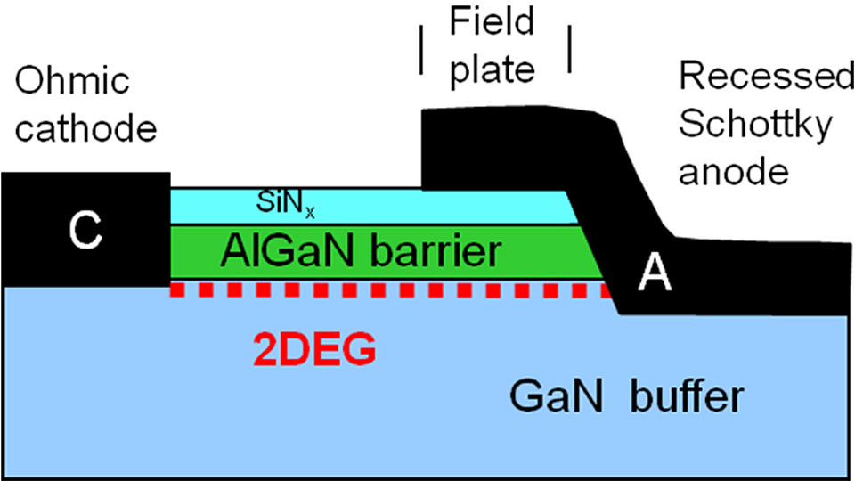
Fig. 1: Schematic cross section of lateral Schottky diode where the anode directly contacts the 2DEG region by recessing.
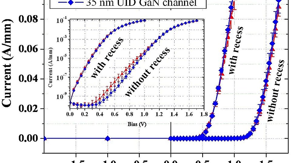
Fig. 2a: Wafer level median diode characteristics of devices with GaN:C back barrier (diode width: 100 µm, anode-cathode distance (LAC): 2 µm). Planar (red) and recessed type of anodes (blue) are compared. Error bars represent the 25% and 75% percentiles. Inset: Log scale plot of the reverse bias regime.
Highly efficient electrical power converters are indispensible for ecology-minded future electronic systems. GaN HEMT power switches are believed to be to mature to one of the most promising technology in this respect. However, in contrast to standard Si-based power switches, the absence of a body diode calls for the development of high-performance diodes that may be used as free wheeling diodes in modern converter topologies. The electrical properties of these diodes such as blocking voltage, turn-on voltage and on-state resistance as well as the switching properties should be compatible to the novel GaN based high-power switching transistors in order to enable inherently efficient converter topologies. In order to meet these requirements, Schottky diodes with lateral device topology have been developed. These devices fully utilize the high channel conductivity provided by the 2-dimensional electron gas (2DEG) at the AlGaN/GaN heterojunction interface. Buffer punch-through of electrons has been avoided by applying an epitaxial buffer design focusing electrons to the channel region using the back-barrier concept as described in [1]. They are thus characterized by low turn-on voltages combined with high blocking capability and high switching speed [2, 3].
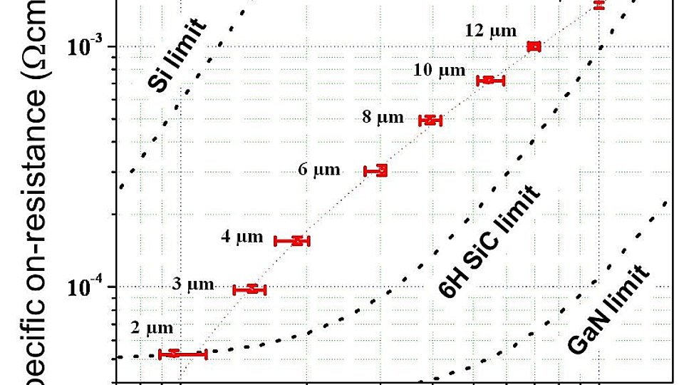
As shown in Fig. 1, the Schottky metal (anode) is placed as close as possible to the 2DEG region by applying a carefully optimized recessing technique. The anode directly contacts the 2DEG region and, at the same time, acts as a field plate which reduces critical concentrations of the electrical field close to the anode. It has been shown that this approach results in a low barrier height yielding a very low turn-on voltage while the blocking capability is not compromised [2, 3]. Fig. 2a shows the wafer level median of the diode forward and reverse characteristics for different versions of the Schottky anode technology. As compared to planar-anode diodes, recessed‑anode diodes show a significant reduction of diode onset voltage from 1.2 V to about 0.46 V (measured at a current level of 1 mA/mm) independent of anode‑cathode separation. This is believed to be due to the reduction of Schottky barrier height to 0.46 eV only if the anode metal is brought into direct contact with the 2DEG after anode recessing according to Fig. 1. In contrast to Schottky diodes on bulk semiconductors, a lower Schottky barrier does not compromise breakdown voltage. Obviously, a significant part of the 2DEG channel region will be depleted at reverse bias conditions. This explains the good scaling of the diode breakdown voltage with increasing anode-cathode distance LAC as depicted in Fig. 2b. A quadratic dependence of the reverse blocking voltage on LAC, is observed (practically ideal Schottky diode behavior). The on‑state resistance of the devices has been calculated to 5.2 × 10‑5 Ω cm2 and 1.5 × 10‑3 Ω cm2 for LAC values of 2 µm and 15 µm respectively. The maximum forward current level at these device dimensions is 0.9 A/mm and 0.4 A/mm respectively. Devices with LAC ≥ 15 µm exceed reverse blocking bias of 1000 V. It has to be noted that these high breakdown voltages can only be obtained if the anode structure additionally acts as a field plate and thus spreads out electrical fields in the vicinity of the anode metal / semiconductor interface [1].
Publications:
[1] E. Bahat-Treidel et al, "<link /fileadmin/fbh-berlin/english/ver08/pub83.htm _blank internal-url-new-window>Punchthrough-voltage enhancement of Al-GaN/GaN HEMTs using AlGaN double-heterojunction confinement", IEEE Trans. on Electron Devices; 55(12), pp. 3354-3359 (2008).
[2] E. Bahat-Treidel, O. Hilt, R. Zhytnytska, E. Cho, J. Würfl, G. Tränkle, "AlGaN/GaN/GaN:C back‑barrier Schottky diodes for power switching", Proceedings of the 35th Workshop on Compound Semiconductor Devices and Integrated Circuits, ISBN 978-88-8080-123-8, pp. 165-166, (2011).
[3] E.Bahat-Treidel, O. Hilt, R. Zhytnytska, E.Cho, J. Würfl, G. Tränkle, "GaN-Based Schottky diodes with low onset voltage and strong reverse blocking", Abstracts of the 38th International Symposium on Compound Semiconductors – ISCS 2011, pp. 246-247, (2011).
FBH research: 07.07.2011


