Gain-switched electrically pumped VECSEL for picosecond pulse generation at 1030 nm
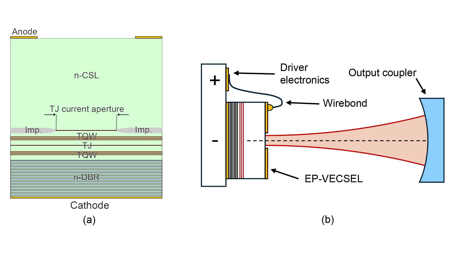
Fig.1: (a) Schematic diagram of a double-stage RPG EP-VECSEL showing the electrical aperture created in the TJ above the topmost TQW and stacking of two active regions with another TJ between them, (b) diagram of the EP-VECSEL in laser operation in a confocal configuration.
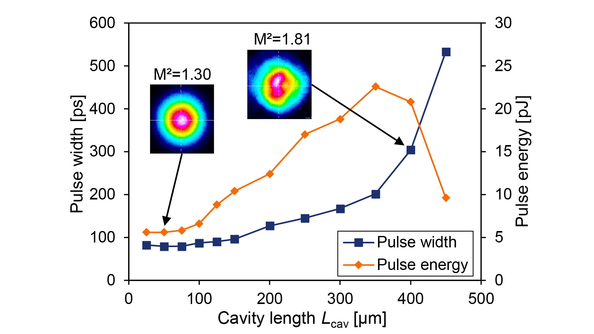
Fig. 2: Pulse width and energy of a 20 µm aperture EP-VECSEL at varying cavity lengths under gain-switched operation (data provided by LZH).
Picosecond optical pulses are of high interest for many distinct applications, including LiDAR, time-resolved spectroscopy, and quantum key distribution. Among semiconductor laser classes, vertical cavity surface emitting lasers (VCSELs) are attractive thanks to their circular beam profiles, which avoid the beam-shaping optics required by edge emitters. For telecom applications, picosecond pulses have been realized via gain-switched VCSELs with a monolithic cavity, which, however, limits true single-mode operation to small apertures (e.g., below 4 µm for oxide confinement) and thus restricts pulse energies.
Vertical external cavity surface emitting lasers (VECSELs) overcome these constraints by decoupling the optical mode area from the electrical aperture. Furthermore, the external cavity provides independent control over photon lifetime via the output coupler reflectivity and cavity length, and over the transverse mode area via the coupler curvature. Ultrashort pulse generation has been demonstrated from both optically pumped OP-VECSELs and electrically pumped EP-VECSELs via passive mode-locking with semiconductor saturable absorbers (SESAMs). The external pump laser in OP-VECSELs, however, limits practical deployment to scientific and niche applications. EP-VECSELs address this limitation, but until recently their repetition rates were very high (216 MHz and higher). Accessing the lower MHz regime required pulse pickers, which increase system complexity.
Here, we report a novel gain-switched EP-VECSEL structure at 5 MHz to generate picosecond pulses around 1030 nm. Gain-switching extracts the first optical spike of the relaxation oscillation, triggered by a current step from below to above the lasing threshold. The structure combines an n-type current spreading layer (n-CSL) grown above two resonant periodic gain (RPG) stages, each containing InGaAs-based triple quantum well (TQW) layers, which are interconnected by a GaAs tunnel junction (TJ). A second TJ is grown between the topmost RPG stage and the n-CSL to prevent the formation of a reverse-biased pn junction and to funnel the current toward the center of the device. The latter is realized by selectively proton implanting this topmost TJ. The implantation triggers diffusion processes during the second growth step, which increases the TJ resistance in the implanted regions. This creates a spatially defined conductivity contrast that confines the current without material etching or lateral oxidation (Fig. 1a). Experimental LED-mode operation results confirm Gaussian electroluminescence profiles for apertures up to 20 µm and uniform flat-top profiles for larger apertures up to 100 µm, indicating homogeneous current injection.
Chips with aperture diameters of 20–100 µm were fabricated at FBH and characterized by our partner LZH (Laser Zentrum Hannover e.V.) under gain-switched excitation. A schematic diagram of the setup is shown in Fig. 1b. The peak drive current was set to 600 mA at a repetition rate of 5 MHz. As shown in Fig. 2, the 20 µm aperture devices produced optical pulses as short as 79 ps (measurement limited by the 10 GHz photodiode bandwidth), with a pulse energy of 5.8 pJ at cavity length Lcav ~ 75 µm with beam quality factor M2=1.3. Increasing Lcav to 350 µm resulted in a maximum pulse energy of 23 pJ at 180 ps pulse width. The M2 factor remained in the range of 1.3 to 2 for Lcav up to 450 µm. Increasing the aperture diameter to 100 µm yielded pulse energies up to 403 pJ, at the expense of increased pulse duration (435 ps).
To the best of our knowledge, this work represents the first gain-switched operation of an EP-VECSEL around 1030 nm. The pulse energies achieved here are well suited for further amplification in Ytterbium-doped solid-state and fiber amplifiers. This positions the demonstrated EP-VECSELs as a compact, electrically driven seed for high-power master oscillator power amplifier (MOPA) systems.
This work was funded by the German Federal Ministry of Research, Technology and Space (BMFTR) within the ED-VECSEL project (contracts 13N16751 and 13N16752) as part of the joint project: “Electrically pumped semiconductor disk laser for ultra-short pulse generation”.