Enabling technologies for more compact InP devices and system integration
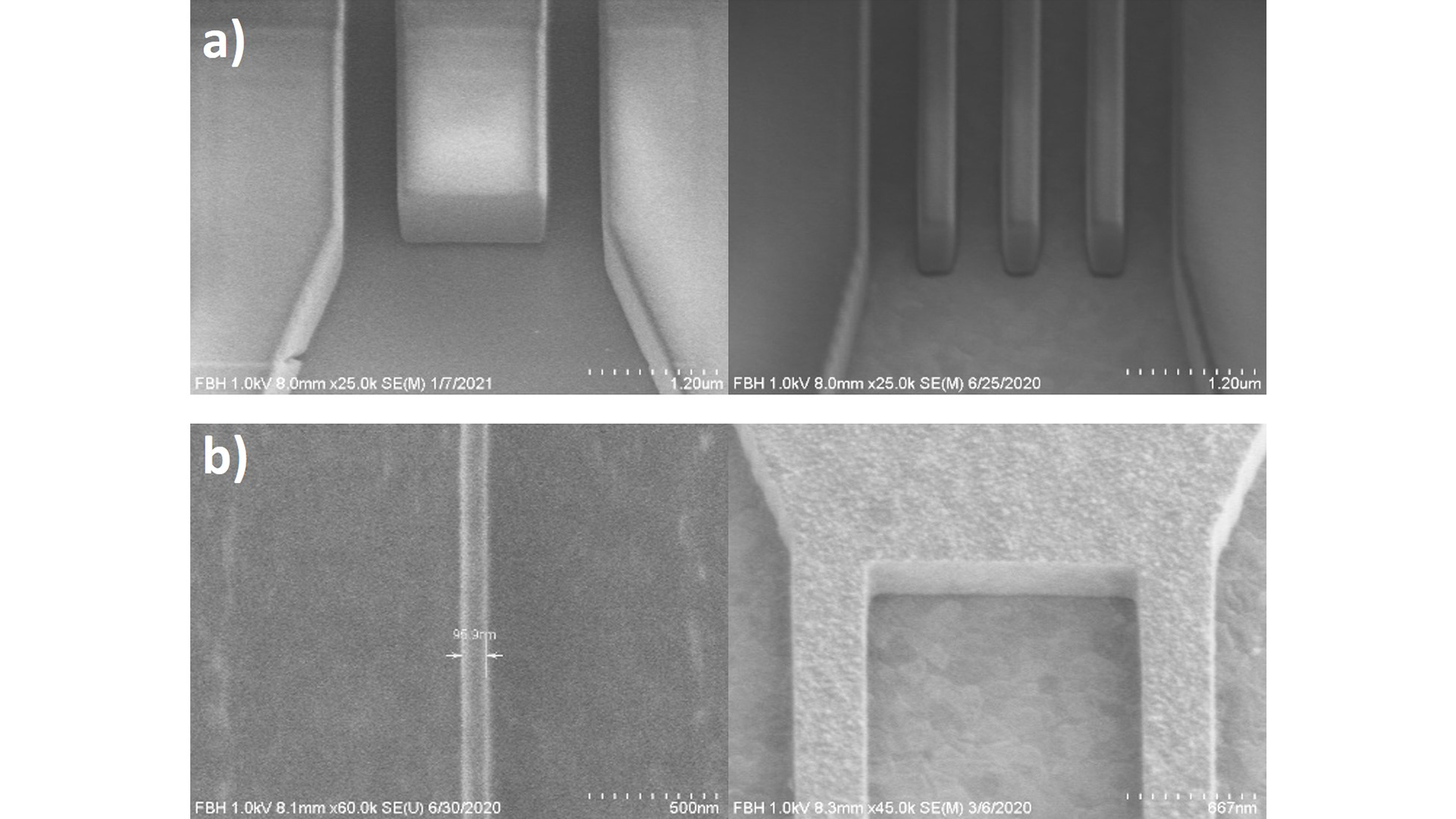
Fig. 1: The SEM images show various writing techniques utilizing the e-beam’s new features to achieve undercut structures (a) or steep sidewalls (b).
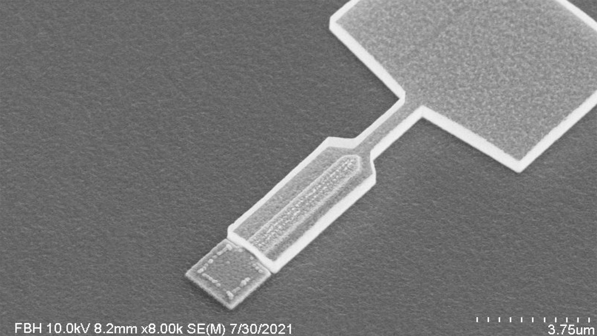
Fig. 2: Processed HBT with 300 nm emitter size decreased from the standard 500 nm node.
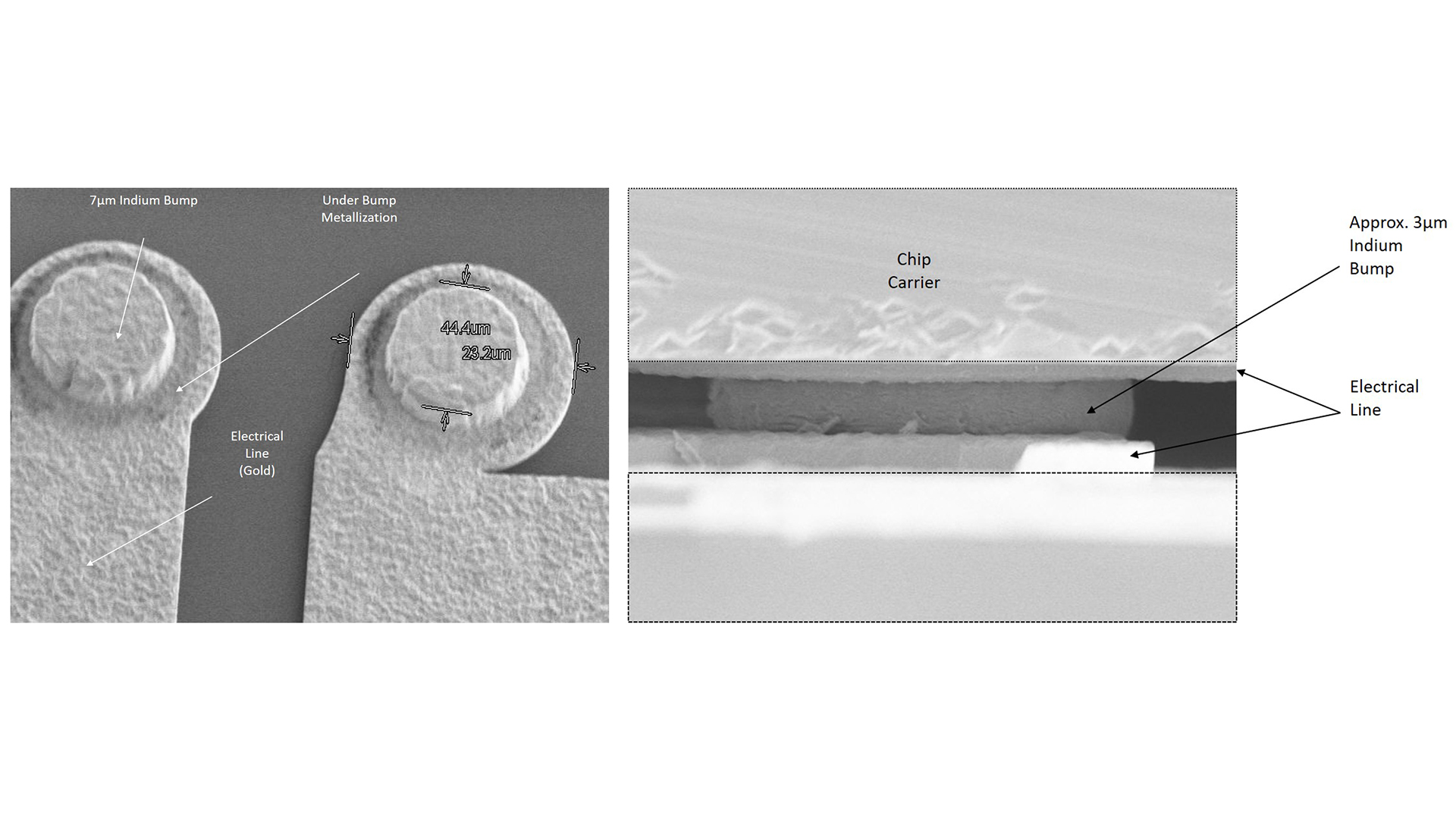
Fig. 3: Flipped circuit on silicon carrier using the novel flip-chip technology with In-bumps.
To integrate InP HBT semiconductor technology in today’s demanding technological landscape, certain requirements have to be met. Firstly, downscaling feature size is inevitable as it leads to higher packing density and design flexibility. Secondly, InP technology must be integrable with existing Si-based technology to ensure a seamless transition, from the concept phase through prototyping to system integration.
FBH maintains the necessary technological prerequisites in its expanded cleanroom capacities with state-of-the-art equipment, thus providing the basis for technological improvements. One example are advancements in InP transistor technology using FBH’s newly acquired e-beam tool.
By the virtue of 100 keV acceleration energy, Raith Ebeam EBPG provides very low scattering of electrons in the resist, even with a thickness of ~1 µm. This leads to vertical sidewalls of the resists, which are required for galvanic deposition and realizing etching masks. However, when using the proximity error correction, one can even achieve an undercut in the resist that is helpful for lift-off processes, see Fig. 1. Such flexibility allows using less resist variations for different processes, which in turn increases yield and throughput.
Utilizing new data preparation tools provided with the e-beam has led to manufacturing a transistor with an emitter size of 300 nm with alignment accuracy below 20 nm, as shown in Fig. 2. The total e-beam writing time of 6 hours reduces the beam time by almost a factor of two with high wafer-to-wafer reproducibility and feasibility of the batch-mode process.
System integration is another important aspect to utilize the advantages of the InP HBT process. Flip-chip technology offers a simple and straightforward solution to be able to place an InP MMIC within a Si-based CMOS environment. Using specially developed In-bumps, a novel flip-chip process has been established at FBH, which allows to integrate circuit chips with a bonding temperature below 220 °C. The low thermal budget of this process makes it appealing not only for InP but for a wide range of different technologies as well. This work is vital in the current project T-KOS as well as the 6G-hub project, which aims at integrating FBHs InP technology with BiCMOs technology from Leibniz Institute for High Performance Microelectronics (IHP) and CMOS technology from Global foundries.
High-end fabrication technology was installed in FBH’s cleanroom thanks to support from the German Federal Ministry of Education and Research (BMBF) provided within Research Fab Microelectronics Germany (FMD). The system integration activities were part of the T-KOS project funded by the BMBF.
The technological prerequisites in the cleanroom were established with funding from the State of Berlin and the European Regional Development Fund (ERDF).