Elaborate assembly technology for tunable diode lasers
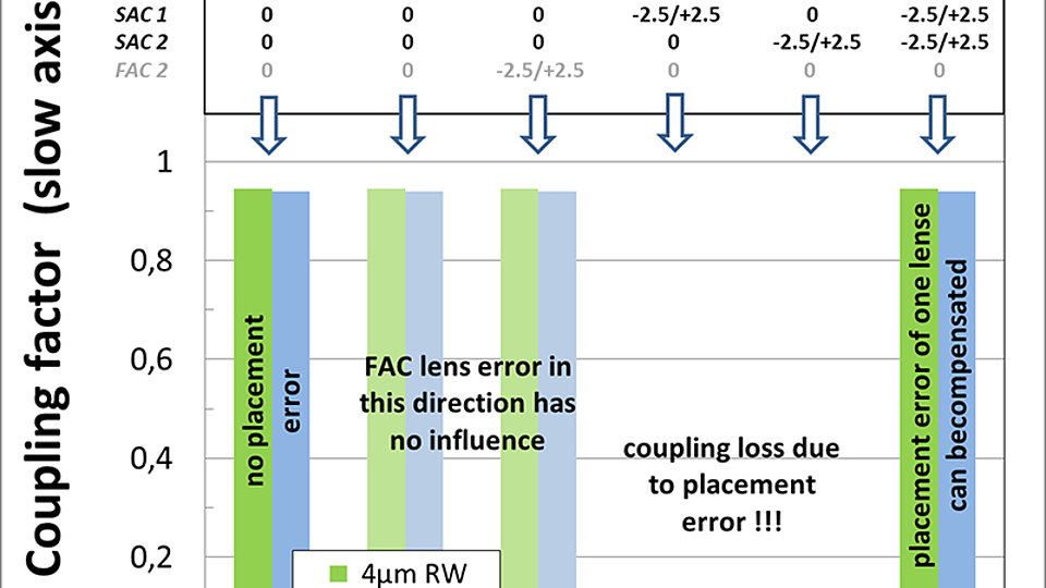
Fig. 3: Simulation results based on an in-house developed software of the coupling in slow axis with placement errors of the different lenses
Tunable diode lasers emitting in the near infrared spectral range are needed in several applications, such as absorption spectroscopy, bio-medical imaging, terahertz frequency generation, and particularly in frequency conversion applications. The FBH develops the suitable light sources for these applications, offering high output power and diffraction limitation along with a tunable narrow linewidth.
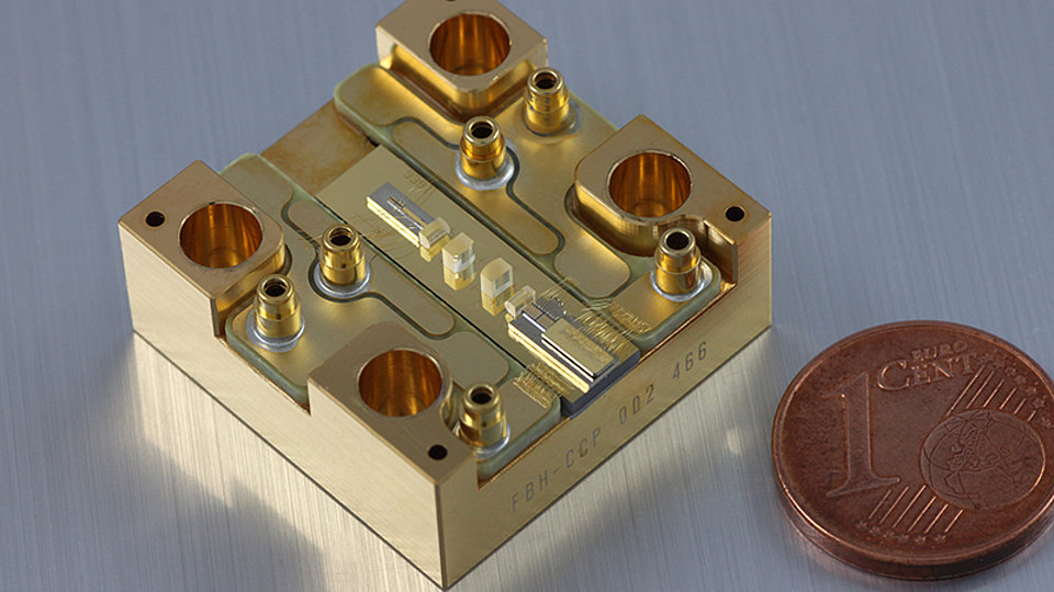
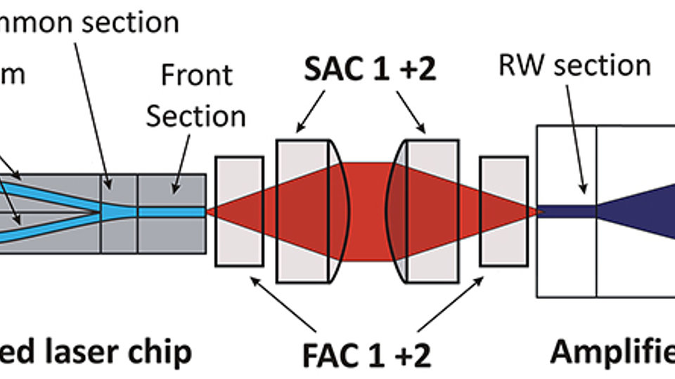
To meet these demands, a master oscillator power amplifier concept (MOPA) is used at FBH, where a seed laser (MO) is mounted in a defined distance to an amplifier laser chip (PA) - so that the generated signal is thermally decoupled from the amplification [Fig. 1]. This leads to a more sophisticated mounting and assembling process, where the goal is to couple the laser light, e.g. from a RW laser section of 2 to 5 µm width into an another small laser section of 2 to 5 µm width over a distance up to 40 millimeters [Fig. 2]. That is, the seed laser light is coupled over at least four lenses (FAC1; SAC1; SAC2 and FAC2) into the amplifier chip.
To guarentee sufficient coupling, basically three options are possible. The first is a full active aligment of the components, represented in principle in the first colomn pair of the diagram [Fig. 3]. Here, a high placement accuracy is reached via directly aligning direction and shape of the laser beam. This means that a beam measurement is essential, and complex algorithms are needed to automate this process. As a result, a manual and time consuming placing by an operator has to be performed in many cases.
The second option is passiv aligment, which is, in general, much faster und can easily be integrated into an automatic placement process, compared to active coupling. On the other hand, a bonding tool with a very high placement accuracy is needed (< 1 µm) to meet the demands, which can be seen in the the fourth und fifth colomn pairs of the diagram in Fig. 3.
The third option is a combination of active and passive alignment, which means, depending on the reached placement accuracy, the possible components are placed first passively. To compensate the resulting error the remaining components are placed actively, which is represented by the last colomn pair in the diagramm of Fig. 3, where, to give an example, a concrete placing error in direction vertical to the beam of +/-2.5 µm can be compensated with the second corresponding SAC lense.
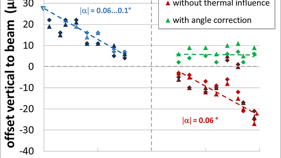
Consequently, it is possible to meet the FBH placement accuracy as can be seen in Figs. 4 and 5 (green dots). Both directions – vertical to and in direction of the beam – have a nearly constant offset of about +/-2.5 µm over several distances.
To reach such a placement accuracy, more than the standard bond parameters like pressure, time and bond temperatur have to be controlled. One of the additional factors is thermal expansion due to a temperature gradient in the bonding process. This leads, especially for the soldering process, to a naerly constant rising error of several µm by an increase of the distance [Fig. 4]. Another important influencing factor is the bond tool itself. It has been demonstrated that a tilting error of a few hundredths of a degree, e.g. 0.06° in this particular case, also leads to a relevant deviation in vertical direction. [Fig. 5]
Future optimizations are expected to further increase the resulting placement accuracy to values of < 1 µm. This should pave the way to placing all components passively in the future.


