Discrete Supply Modulated (class-G) MMICs for Space Applications and 5G
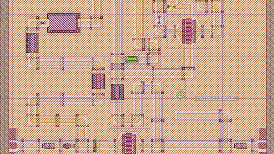
Fig. 1: MMIC class-G amplifier based on 12x50 μm transistors with voltage switch, designed for operation in the 20-26 GHz range
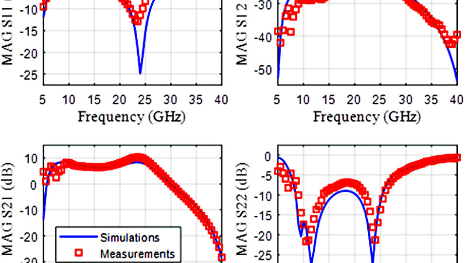
Fig. 2: Small-signal S-parameters comparison at 28 V with IDQ = 145 mA. Simulated results for the MMIC are shown in solid lines, measurements as red squares
In recent years, the focus of FBH’s RF Power Lab has been to transfer the knowledge and methods for efficiency enhancement implemented in discrete RF power GaN technology to integrated MMIC solutions for higher frequency applications. This is challenging in many aspects: designs are model-based and post-fabrication tuning is impossible. Furthermore, there is a large delay from design to fabrication and evaluation. Mainly the discrete level supply modulation, i.e. class-G, shows promising performance for the upcoming large instantaneous modulation bandwidth and will be the future main focus of the work.
A first MMIC design with integrated class-G modulator [1] was a single-stage amplifier based on a 12x50 µm GaN HEMT fabricated in the 150 nm in-house technology. The single-stage amplifier was developed for tests in the 18-20 GHz space communication band and the first mmW band for 5G at 24-26 GHz. The MMIC layout shown in Fig. 1. includes the power amplifier, a voltage switch based on a similarly sized transistor, and a GaN diode to supply the lower supply voltage when the transistor switch is open. The control of the switch with the digital isolator and the gate driver is designed off-chip but some stabilization of the switch is implemented on the MMIC. The well-known discrete GaN diodes from the FBH have now been adapted to the MMIC process and are available for integrated solutions. The small-signal evaluation in Fig. 2 shows good agreement with simulated results, indicating accurate modelling and stability in the process since the models are based on a previous run. Large-signal measurements at various supply voltages measured over the diode show an output power of 30.8 dBm at 20 V supply voltage in 3 dB compression. This is equal to 2 W/mm gatewidth. Reducing the supply voltage from 28 V to 8 V decreases the output power and reduces the gain considerably from 7.2 dB to 4.9 dB. The quasi-static evaluation shows that at an output power of 26.6 dBm can be produced at 28 V supply with 12% drain efficiency or at 8 V supply with 40% drain efficiency, but with a much reduced gain.
Post processing using a 10.6 dB PAPR OFDM signal and a peak 1 W output power shows a possible drain efficiency improvement of 10%-points (from 5% to 15%) with a 2-stage class-G modulator operating at 8 V and 20 V. Space applications in the 20 GHz range use less complex modulation formats and allow much larger compression of the output signal where class-G has a much lower improvement potential. Even so, post processing of the CW data shows a possible efficiency improvement of 7%-points (from 16% to 23%) for the MMIC for a 3 dB PAPR signal. All calculations are based on a loss-less modulator. At present, an improved gate driver is in development to allow dynamic characterization of the MMIC with a bandwidth in the 500 MHz range.
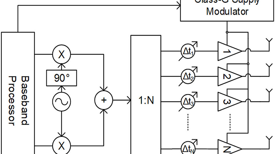
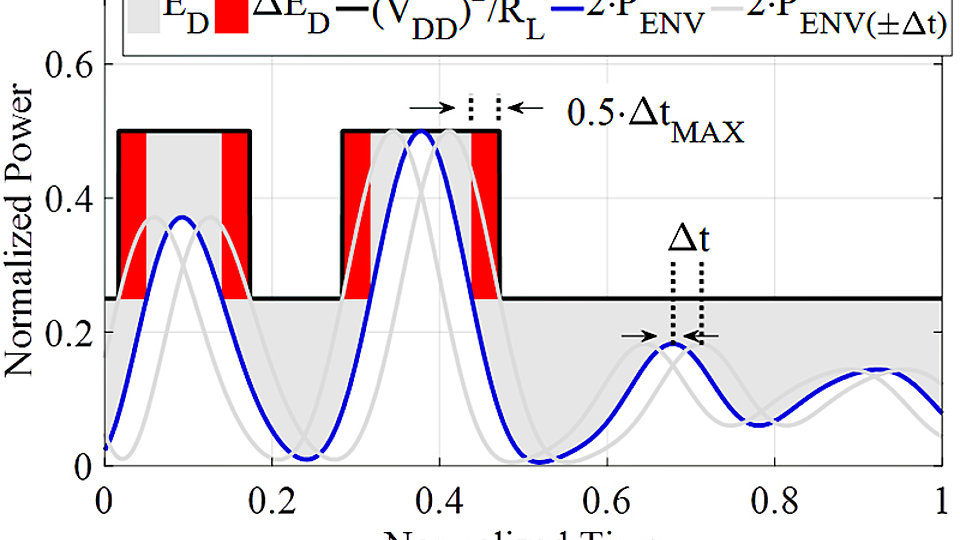
Given the low power of each cell and the large power dissipation in the gate driver it is unlikely that future systems based on array amplifier structures can afford an individual modulator for each amplifier. Therefore, a less complex PA architecture for beam-forming has been investigated [2], which is shown in Fig. 3. Here, one supply modulator provides the discrete voltage levels for all PAs in the array. To avoid compression of some PAs, the pulsewidth of the high-state of the discrete level supply has to be extended to cover the high-power states of all amplifiers in the array. The high supply voltage pulses must be expanded by ΔtMAX, which is a function of the beam-forming angle and the physical size of the antenna, i.e., ΔtMAX = Δt(Lx,Ly,Θx,Θy). This is illustrated in Fig. 4 for a system with two supply voltage levels. The investigations, which are based on post processing of data from real dynamic discrete level supply voltage modulation measurements of a single-input-single-output (SISO) PA, show that class-G supply modulation can still achieve improved system efficiency of about 10%-points. However, the linearity quantified by ACLR deteriorates rapidly with delay, which increases with relative modulation bandwidth, number of antenna elements (i.e. size), and beam-angle.
The coming year will show the first dynamic results of discrete level supply modulation implemented for very high instantaneous modulation bandwidths in mmW amplifiers. These achievements will outline the role for high efficiency GaN in future 5G telecom and space applications.
References
[1] GaN-HEMT MMIC with integrated Class-G Switching Stage for Discrete Level Supply Modulation for 20 GHz Space Applications, presented at the Latin American Microwave Conference, LAMC 2018.
[2] N. Wolff, W. Heinrich, O. Bengtsson, "Class-G Supply Modulation for MIMO and Radar with Phased Array Antennas", 12th German Microwave Conference (GeMiC 2019), Stuttgart, Germany, Mar. 25-27, ISBN 978-3-9812668-9-4, pp. 131-134 (2019).


