Development of GaN-based Ka-band MMICs for space communication systems
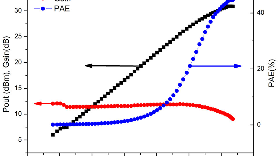
Fig 2: Load-pull measurement results of 4×75 µm-wide transistors fabricated on-wafer with GaN:Fe buffer (@ 18 GHz, VDS = 28 V, tune for max Pout)
The fast development of Ka-band broadband satellite communication systems is mainly driven by the capability of this technology offering high data transmission rates. Ka-band satellite applications require highly sophisticated transceiver MMICs. In particular, highly linear and efficient power amplifier MMICs for the transmitters and low-noise amplifier MMICs for the receivers are indispensable. GaN-MMICs technology is very promising to satisfy these demands.
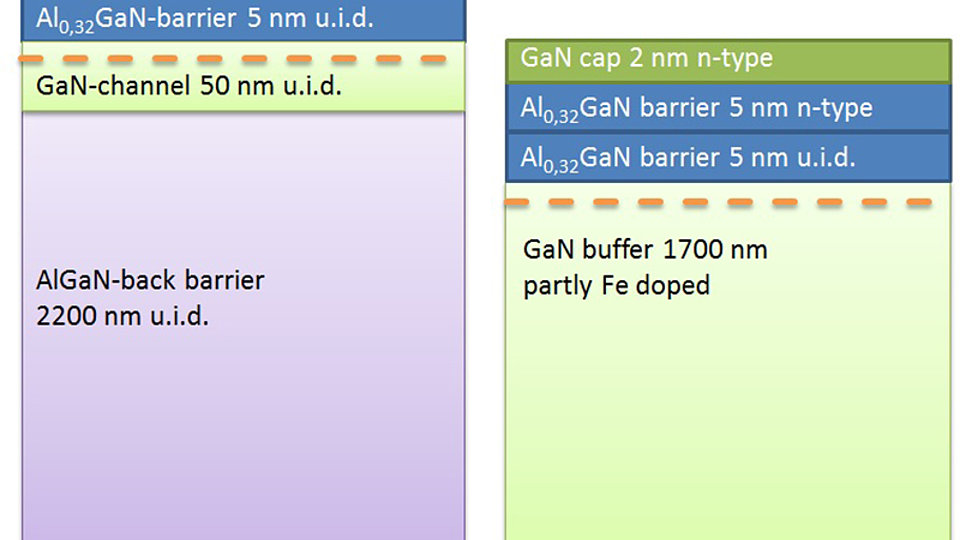
However, both MMIC fabrication process flow and epitaxial structure should be properly optimized for the given frequency range. Compared to existing X-band MMICs, Ka-band MMICs require a reduced transistor gate length (Lg). The epitaxial structure has to be adjusted accordingly to avoid adverse effects related to the reduction of aspect ratio between Lg and gate to channel distance as the gate length decreases (short-channel effect). Recently, the FBH has developed a reliable and scalable technology for the fabrication of embedded gates with slanted sidewalls and lengths ranging from 100 nm to 500 nm. Shorter gates are suitable for the development of Ka-band MMICs. In order to produce Ka-band devices with state-of-the-art characteristics an optimum combination of gate length and epitaxial structure design has to be found. The devices investigated have been fabricated by combining two different epitaxial stacks (Fig. 1) with transistors of gate lengths ranging from 100 nm to 200 nm.
DC measurements show that the epitaxial structure with GaN:Fe buffer layer has a higher drain current density as compared to the epitaxial structure with an AlGaN back barrier (~ 1.0 A/mm and ~ 0.7 A/mm respectively). Fig. 2 displays the Pout/ gain/PAE curves vs. input power as obtained from load-pull measurements at 18 GHz and 28 V drain bias on 4 x 75 µm wide devices with 100 nm gate length. The output impedance has been tuned to the maximum output power Pout. An output power density of ~ 3 W/mm at a PAE of ~ 45% could be obtained. These are state-of-the-art results. Devices fabricated on AlGaN/GaN back barrier epitaxial structures showed lower performance data in terms of Pout, PAE and gain.
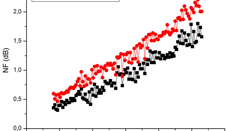
Fig. 3 compares the RF-noise performance of transistors fabricated on epitaxial structures according to Fig. 1. The noise performance of transistors fabricated on-wafer with AlGaN back barrier is better as compared to transistors on-wafer with GaN:Fe buffer. The noise measurements data, extrapolated up to 30 GHz show a noise figure of 1.94 dB for the wafer with AlGaN back barrier in the buffer and 2.29 dB for the wafer with GaN:Fe buffer. The corresponding associated gain is 7.34 dB and 6.46 dB, respectively. The analysis of the large-signal and noise performance evaluation reveals that the epitaxial structure with Fe-doped GaN buffer provides better performance in terms of output power and can be used for the fabrication of power amplifier MMICs for transmitters in Ka-band communication systems. The epitaxial structure with AlGaN back barrier provides better noise figure and is therefore preferable for the fabrication of low-noise amplifiers used as receivers in Ka-band communication systems.
FBH research: 05.12.2014


