D-band up-converter with gain peak conversion of 17 dB using extremely scaled InP DHBT epitaxy
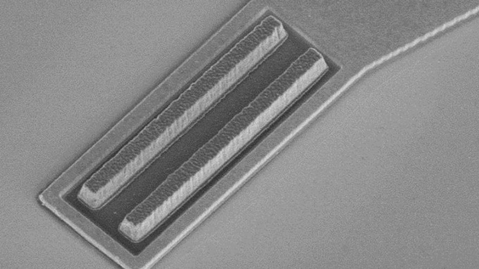
InP-based transistors offer superior performance in the sub/THz range. Sub-micron double heterojunction bipolar transistors (DHBT) were fabricated using a substrate-transfer technique, giving access to the front and back side of the epitaxy. The critical layers were structured using electron beam lithography (EBL) with an alignment resolution of sub 20 nm. This enabled the patterning of highly symmetrical base contacts and centered collector on the emitter. To support a submicron process the device epitaxy was extremely downscaled. This was achieved by significantly reducing the thickness and heavily doping the emitter and base layers. A novel dual-base deposition technique was used to reduce the composite metal sheet resistance. This can be seen from Fig. 1 with the elevated double base metalization process. Before deposition, the junction was treated with H2SO4 and passivated with SiNx afterwards. The ground plane was elevated by using a 700 nm thick emitter notch. Finally, the topmost gold layer was designed to offer both microstrip and coplanar structures for device characterization.
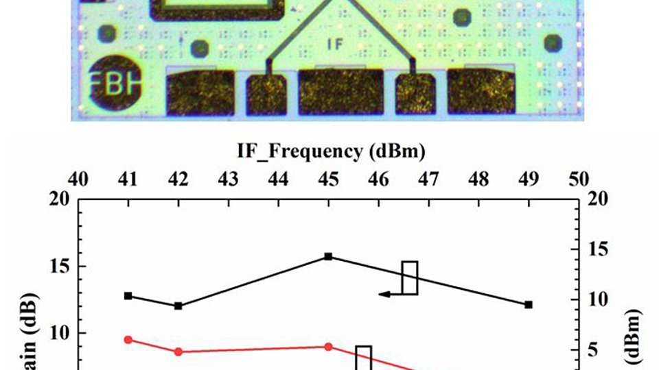
The processed technology demonstrated a D-band (110 – 170 GHz) fundamental frequency up-converter with high conversion gain. The MMIC realized uses an 800 nm wide emitter and achieves ft and fmax values of about 350 GHz with BVCEO = 4 V. The up-converter achieves a single sideband (SSB) peak conversion gain of 17 dB at 145 GHz and > 10 dB in the frequency range 141 – 149 GHz. DC consumption is only 25 mW. Fig. 2 shows a microphotograph and the measured output power and conversion gain of the up-converter chip.
Publication
[1] M. Brahem, H. Yacoub, K. Nosaeva, N. Halder, N. Kemf, S. Seifert, G. Tränkle, "The Effects of Device Scaling on the DC Performance of Deep Submicron Transferred-Substrate InP/InGaAs DHBTs", Compound Semiconductor Week 2020, Stockholm, Sweden.

