A unique tool for sputtered iridium gate technology
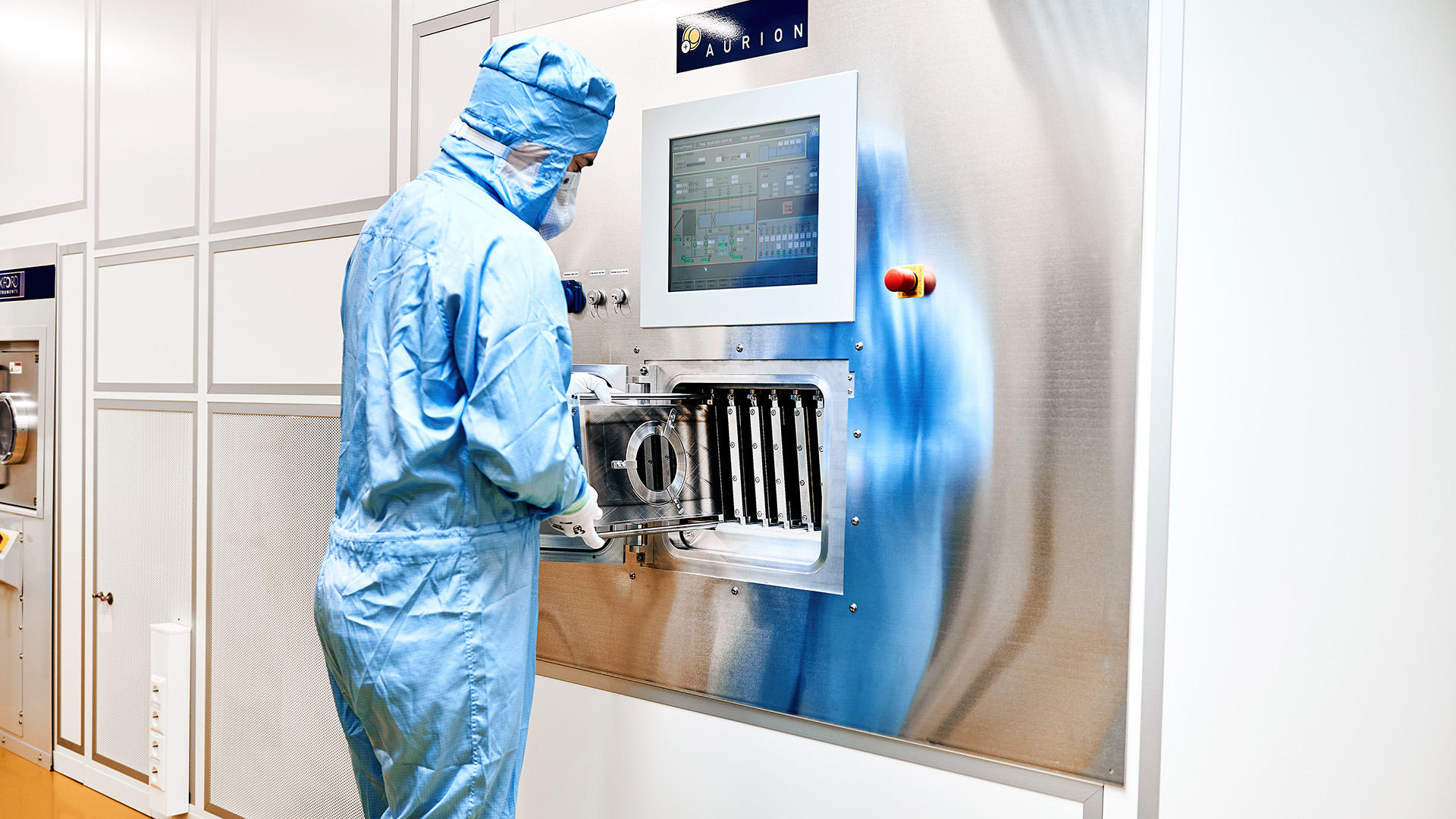
Fig. 1: Loading the sputter tool with 100 mm wafers clamped on carriers.
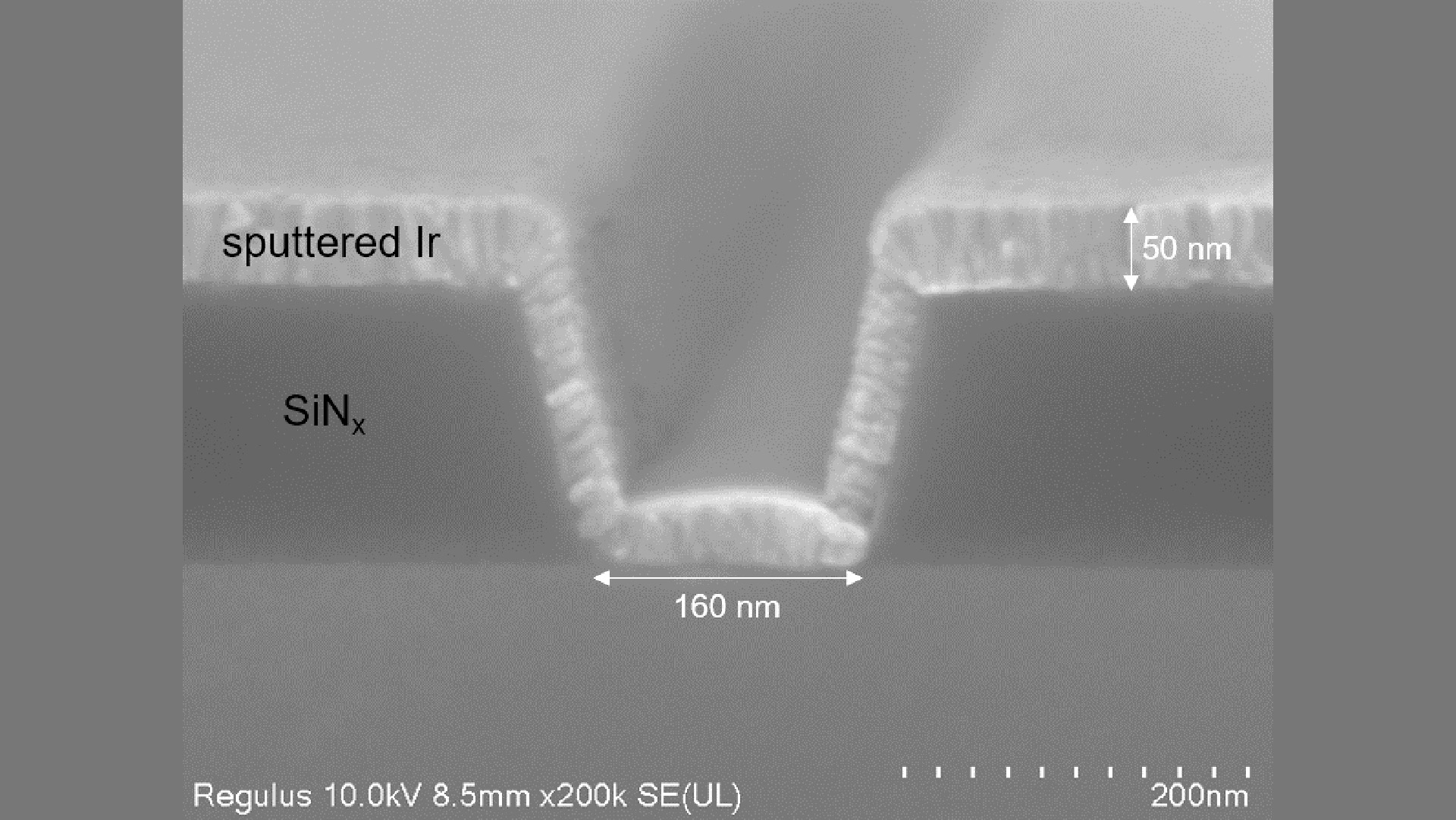
Fig. 2: Gate trench etched in silicon nitride, covered with sputtered iridium.
FBH has put a new sputter tool into operation that is based on the principle of a quasi-vertical deposition process. This tool was tailored to fit the needs of the sensitive iridium sputtering process of FBH’s transistor gate technology. It helps to further advance the development of GaN MMIC devices and ensures a cross-contamination free process.
FBH's GaN MMIC process is based on a sputtered iridium gate technology as Schottky barrier metal. This worldwide unique technology significantly reduces dispersion effects and increases the long-term reliability of the active components. It is based on a sputtering process that significantly reduces the level of contamination, since the sensitive gate process determines the final device performance. Most commercially available sputtering systems implement a horizontal sputtering process. In this case, the wafer is either placed at the bottom and the sputter target positioned above it or the target is located at the bottom and the wafer to be processed is placed above and faced upside down. With regard to cross-contamination, both options are not optimal.
FBH is therefore pursuing the concept of a quasi-vertical sputtering system developed together with the German system manufacturer Aurion Anlagentechnik GmbH. Here, the substrates are vertically aligned with a 7° tilt angle. In this way, the generated particles do not interfere while simultaneously the substrates are securely held in pockets on carriers. Batches of up to 6 wafers can be loaded, which are processed sequentially (see Fig. 1). The wafers first pass through a preparation chamber in which the substrates can be heated or sputtered with argon for in situ pretreatment. The main chamber contains four DC-magnetrons. In addition to iridium, the equipment also allows to sputter TiW (10:90wt%) and gold, e.g., to deposit seed layers for plating applications. Since iridium layers are sensitive to oxygen and moisture that deteriorate the film properties in terms of conductivity, the tool is equipped with cryogenic pumps which enable efficient moisture removal.
To apply sputtered iridium as a Schottky barrier metal in the GaN gate process, conformal coating of etched gate trenches is important. Fig. 2 shows a sputtered iridium film in an etched gate trench with 160 nm gate length. The film is continuous, smooth and without any voids. The sputtered iridium film exhibits a good top-to-bottom conformality of 78% and a top-to-side conformality of 57%. To further improve the step coverage of the thin film, an additional HF bias can be applied to the wafer. By superimposed back-sputtering, the step coverage of the film can be further optimized.
We gratefully acknowledge financial support by the German BMBF within the "Research Fab Microelectronics Germany (FMD)" framework under ref. 16FMD02.