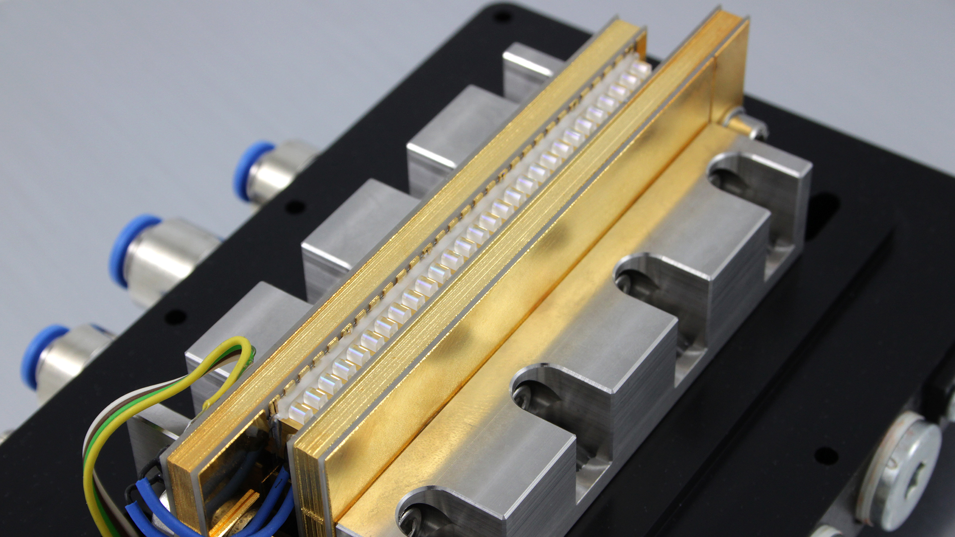
Applications
- Remote sensing
- Illumination
- Pumping of solid state, fiber and gas lasers
- Measurement and control engineering
- Medical technology
- Sensors
- Material processing
Wavelength
630 nm to 1200 nm
Chip technology
- Semiconductor layers by means of MOVPE
- Monolithic gratings via surface etch technology or two step-epitaxial techniques
- Contact windows by
- projection lithography
- implantation and isolating layers
- deposition of metalization
- Thinning
- Scribing, breaking and cleaving
- Facet coating and passivation with extremely long lifetimes
Assembly
- Hard, gold-tin soldered packaging
- Open heat sinks (C-Mount)
- Conduction cooled package (CCP)
- Expansion matched submounts
- Integrated double-side heat-sinking
- Additional FAC lenses (fast axis collimator) and external gratings possible
Typical data
- NIR range:
- up to 30 W cw output power depending on wavelength and geometry [publication]
- up to 60 W output power in quasi-continuous wave mode (1 ms pulse width, publication)
- peak power density of over 110 MWcm-2 driven by short pulse source [publication]
- conversion efficiency > 65% at 10 W output from devices with 90 µm emission aperture [publication]
- 10 W reliable output power from monolithically grating stabilized devices with 90 µm emission aperture [publication]
- high power laser with vertical far field of < 16° (95% power content, publication)
- 17 W near-diffraction-limited emission from a single semiconductor light source [publication]
- reliable output power >120 W (1 ms 200 Hz) from an aperture of 1.2 mm [publication]
- up to 7 W output power from a 30 µm aperture, with a beam parameter product of < 2 mm mrad [publication]
- Red spectral range:
- up to 1 W output power at 635 nm
- high efficiency of 37 % at 635 nm [publication]
- 654 nm devices with 2.7 W reliable output (100 µs 35 Hz, publication)
- 670 nm devices with 1.2 W reliable cw output power [publication]