Tuning surface properties of dielectrics on InGaAs: on the passivation of InP HBTs for high-frequency devices
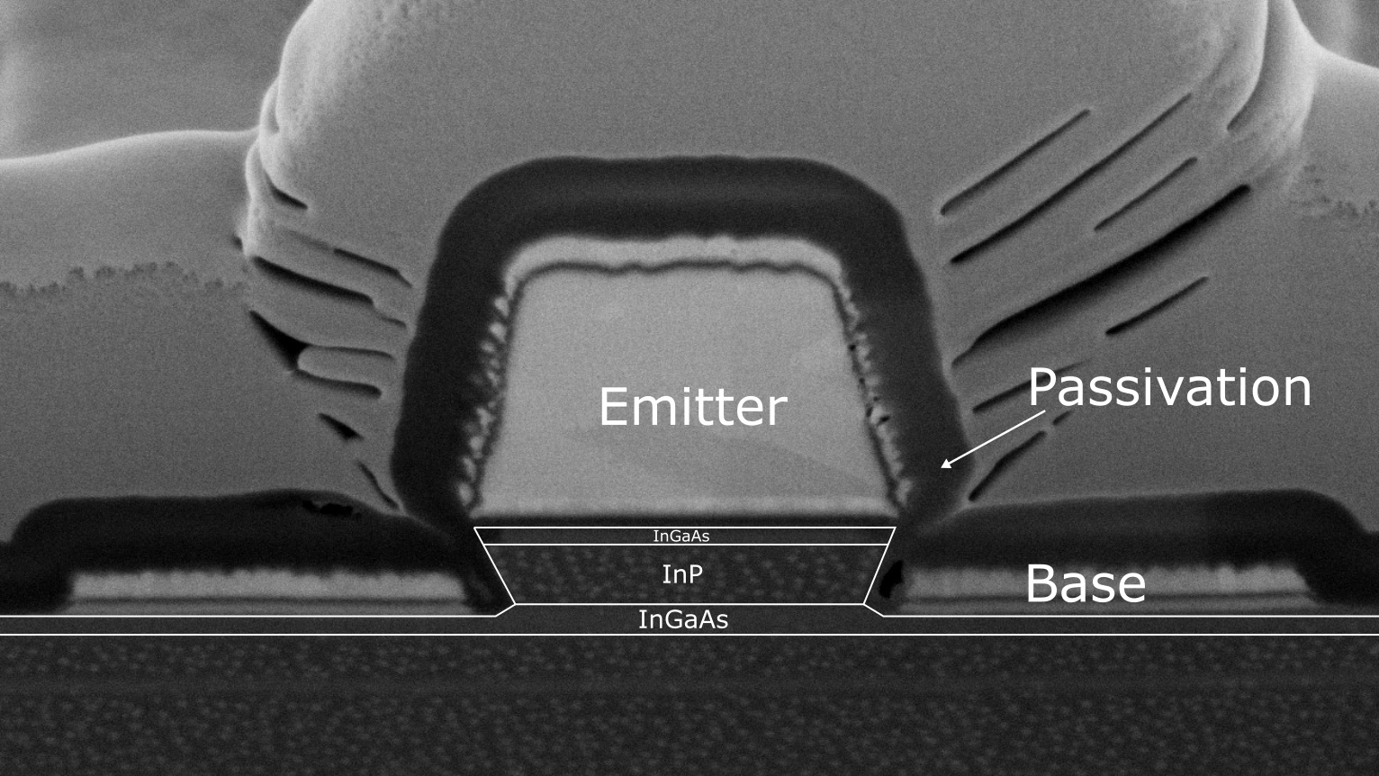
Fig. 1: FIB cross-section of passivated transistor with highly conformal AlOx.
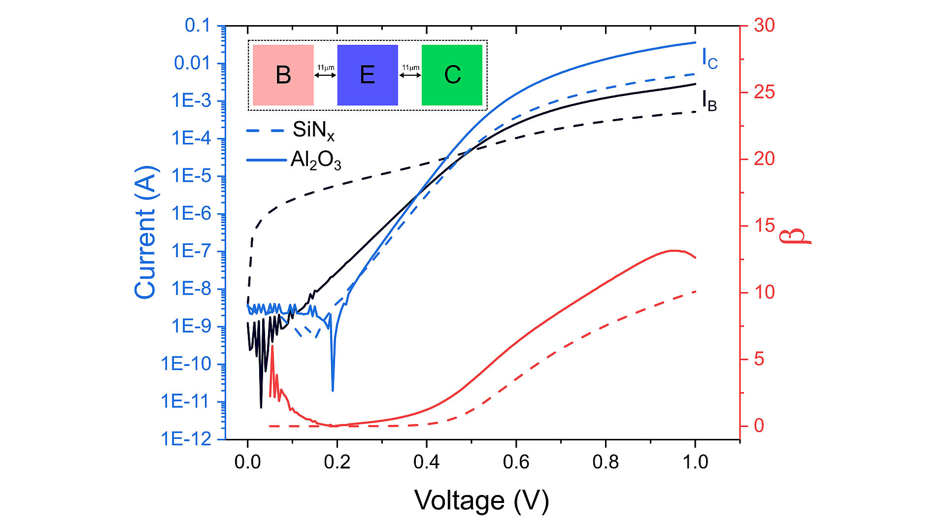
Fig. 2: A comparison of the Gummel plots of two large area transistors (LATs).
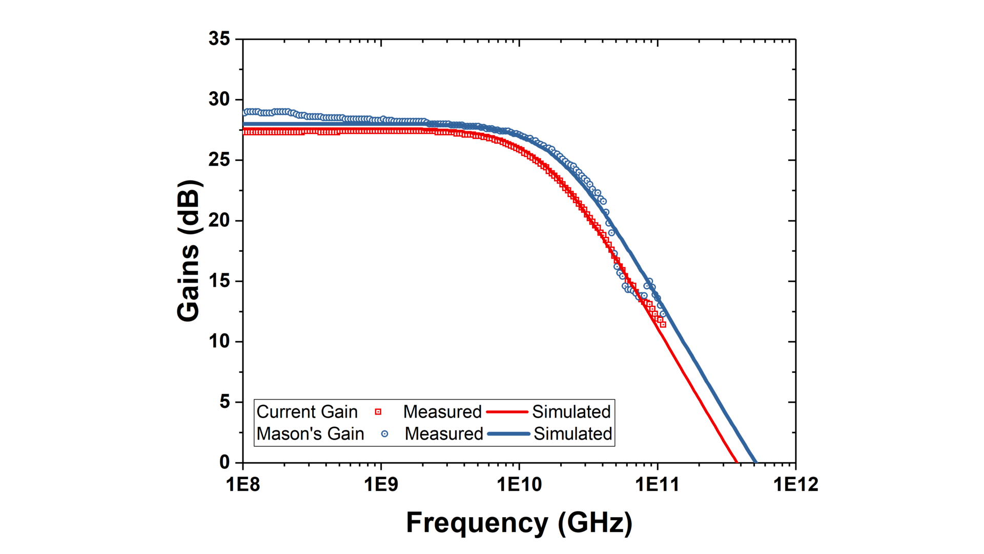
Fig. 3: Current gain and Mason’s gain of a 400 nm transistor with AlOx passivation.
The excellent high-speed performance of InP HBTs makes them particularly interesting for high-frequency electronics. High maximum unilateral power gain frequencies fmax of up to 1 THz have been demonstrated, with power amplifiers operating at frequencies > 100 GHz. Critical to realizing high-performance InP/InGaAs HBTs is the passivation of the InGaAs base layer.
The aggressively scaled nature of this layer, which improves device performance by reducing base recombination current, necessitates the fabrication of high-quality InGaAs/passivation interfaces. Undefined surface states and defects at this interface will reduce the HBT performance by increasing recombination rates, including compensation effects, and raising the base resistance.
FBH has extensive expertise and a large portfolio of dielectric deposition methods which allow the exact tuning of surface properties to accommodate various device needs. For the InP HBTs, we opted for a novel thin atomic layer deposited AlOx film. This approach allows full conformal coverage of the transistor with minimal thickness and can be implemented at significantly lower temperatures than comparable plasma-based deposition methods displayed in Fig. 1.
To evaluate the effect of this novel passivation method on the device properties, we developed dedicated test structures. These structures amplify the influence of surface passivation whilst requiring only minimal processing steps. Large area transistors (LATs) were fabricated, measured, and compared for the standard and the new passivation approach. This strategy allowed a larger sample size and facilitated optimization of the passivation layer thickness and surface pretreatment.
For the optimized passivation process, the test devices exhibited a significant improvement in the current gain factor “ß”, lower leakage current, and a lower current cross-over point seen here in Fig. 2. These results indicate more effective surface passivation with fewer surface states. Using the optimized surface passivation process, resulting scaled transistors have shown improved RF performance, with ft reaching 370 GHz and fmax of 510 GHz as depicted in Fig. 3.
In summary, utilizing tailored low-temperature ALD AlOₓ passivation enables effective control of surface-related effects in scaled InP/InGaAs HBTs and supports their use in millimeter-wave and sub-terahertz applications.