On-Chip Optical Components
Real-world quantum devices require low-loss chip-based optical components to be interfaced with quantum emitters in a robust manner. Starting point of the chip fabrication is the design of low-loss waveguides and high Q cavities with the aim to realize geometries that combine facile fabrication with appropriate single-mode propagation and confinement. Special emphasis lies on the realization of a robust interface for fiber coupling and on the spatial and spectral matching to the emitter of choice.
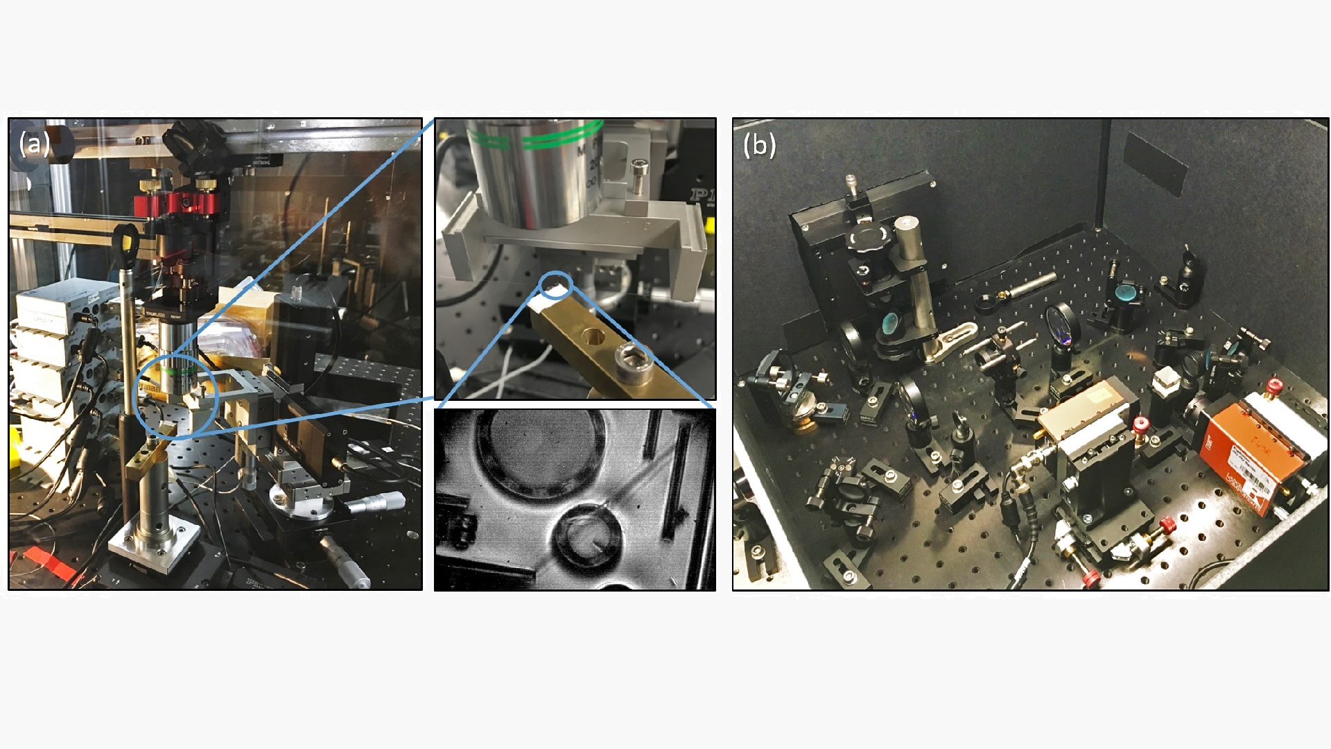
The chips are fabricated in the cleanroom facilities of FBH and then characterized and optimized by the Joint Lab team. Optical characterization of the chip-based optical components and quantum emitters is carried out with custom-made setups for coupling light into and out of chip-based components via a piezo-driven approach of nanofibers. A confocal epifluorescence setup is used for the characterization of quantum emitters.
Apart from the numerical optimization of the geometries, surface optimization of the photonic components will be carried out by ion beam-based polishing using focused beams of helium, neon or gallium. Focused ion beams will be further employed for rapid prototyping of novel photonic component geometries in a close feedback loop to numerical modelling.
Finally, deterministic coupling of quantum nonlinearities to on-chip components constitutes the major challenge of the project. Here, different protocols will be explored like, e.g., the pick-and-place transfer of molecular emitters in a crystalline matrix and of luminescent defects in 2D materials or the co-integration of chip fabrication with ion beam-based defect creation.
This Joint Lab project is carried out in close collaboration with the Fundamentals of Optics and Photonics group of Prof. Arno Rauschenbeutel at Humboldt University Berlin.