Optimization of Te-doped GaAs tunnel junctions for stacking of multiple laser sections
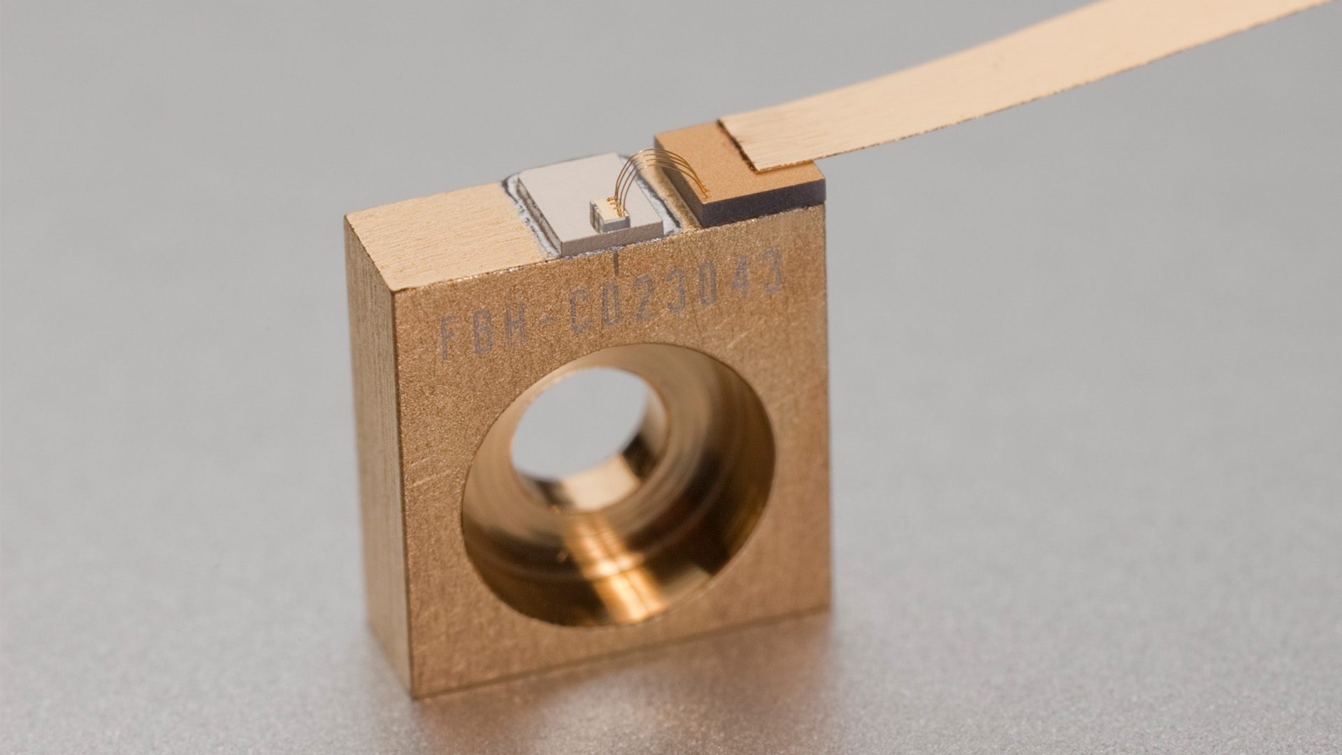
Mounted laser diode
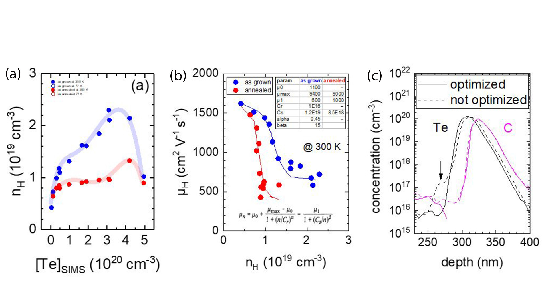
Fig. 1. Hall Data of as grown (blue) and annealed (red) GaAs:Te layers at room temperature (a) free electron concentration nH vs. Te concentration [Te]SIMS and (b) Hall mobility µH vs. nH. (c) SIMS profiles of Te and C in GaAs for samples grown under optimized (black) and unoptimized (cyan) conditions.
Tellurium (Te) as group VI element is of interest as n-type dopant in III-V compound semiconductors, since it is not amphoteric like the group IV dopants silicon (Si) and germanium (Ge). In particular, it has been used to achieve highly doped n++-type layers for tunnel junctions (TJ), electrically connecting different stages in multijunction solar-cells. At FBH, GaAs:Te/GaAs:C tunnel junctions are of interest to stack multiple active regions in laser diodes. While tunnel junctions are usually grown at low temperatures to allow high Te and C incorporation, subsequently grown AlGaAs layers with high Al content favor higher growth temperatures. Furthermore, the Te incorporation into subsequent active layers can deteriorate the device performance due to segregation. Thus, the thermal stability of GaAs:Te and the Te incorporation near the TJ have been studied and optimized to allow for reliable application in light-emitting devices with multiple stages.
All samples were grown in a 12 x 4" planetary MOVPE reactor (AIX2800G4) on exact (100) semi-insulating GaAs substrates from TMGa and AsH3 using diethyl-tellurium (DETe) and carbon tetrabromide (CBr4) as dopant sources for n- and p-type doping, respectively. In the first experiment, several single layer samples with GaAs:Te layers of 100 nm to 200 nm thickness were grown at a low temperature (560 °C). In order to simulate the subsequent growth of AlGaAs layers at elevated temperature, selected samples were annealed at 740 °C for 30 minutes under As-rich conditions using the same reactor. The combination of carrier concentration from Hall data with the incorporated Te content [Te]SIMS from SIMS results from the as grown and annealed samples (Fig. 1 a) reveals free electron concentrations nH of up to 2 x 1019 cm-3 (as grown) and 1 x 1019 cm-3 (annealed) for [Te]SIMS exceeding 1 x 1020 cm-3, which corresponds to an activation < 10 %. The pronounced reduction in carrier activation is very likely due to the formation of acceptor-like species such as the native point defect VGa3- or complexes like (VGa-TeAs)2- [1]. The decrease of the carrier mobility (Fig. 1 b) from 1600 cm²/(Vs) to 500 cm²/(Vs) with increasing nH can be fitted in very good agreement using an empirical relationship from Ref. [2]. Under optimized growth conditions, the Te content steeply decreases by four orders of magnitude over only 25 nm minimizing impact on subsequently grown active regions. (Fig. 1 c).
In conclusion, tellurium offers higher maximum carrier concentration than possible with Si. Also, it does not show fast diffusion like Si when incorporated at levels above 2 x 1018 cm-3 [3]. In the process design including tunnel junctions with Te-doped n-side (a), however, thermal deactivation of the electrical performance of GaAs:Te in the TJ during further growth were considered and (b) proper growth conditions were chosen to reduce Te carry-over into subsequently grown layers. As a result, laser diodes with three stacked active regions electrically connected by two tunnel junctions and emitting into a common optical mode [4] could be successfully fabricated.
The work has partially been funded by the German Federal Ministry of Education and Research (BMBF) within the WelStaMu project under the project reference 13N15566.
Publications
[1] D. L. Williamson et al., “Nature of defects in heavily Te-doped GaAs,” Revue de Physique Appliquee, vol. 18, no. 8, pp. 475–478, 1983, doi: 10.1051/rphysap:01983001808047500.
[2] G. Masetti, M. Severi, and S. Solmi, “Modeling of carrier mobility against carrier concentration in arsenic-, phosphorus-, and boron-doped silicon,” IEEE Transactions on Electron Devices, vol. 30, no. 7, pp. 764–769, Jul. 1983, doi: 10.1109/T-ED.1983.21207.
[3] T. Ahlgren, et al., “Concentration dependent and independent Si diffusion in ion-implanted GaAs,” Phys. Rev. B, vol. 56, no. 8, pp. 4597–4603, 1997, doi: 10.1103/PhysRevB.56.4597.
[4] H. Wenzel, A. Maaßdorf, C. Zink, D. Martin, M. Weyers, A. Knigge, ”Novel 900 nm diode lasers with epitaxially-stacked multiple active regions and tunnel junctions,” Electronic Letters vol. 57, no. 11 pp. 445-447, 2021, doi: 10.1049/ell2.12162.