Optimization of epitaxial growth based on photoluminescence
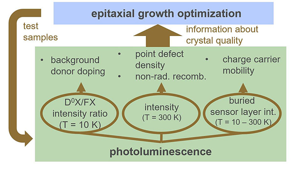
Fig. 1: Photoluminescence provides feedback for optimizations in epitaxial growth of III-V semiconductors.
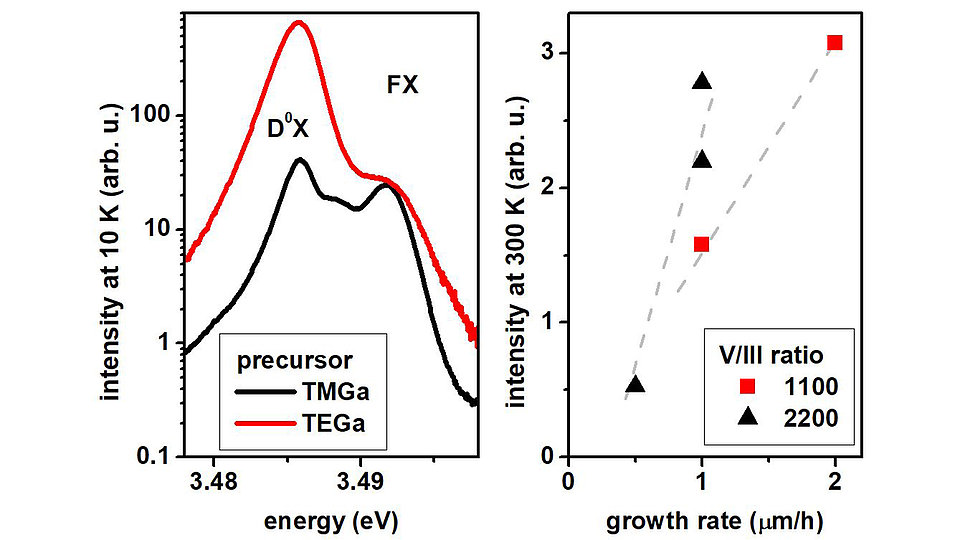
Fig. 2: Low temperature photoluminescence (PL) with high spectral resolution (left) yields information on background doping. Room temperature PL intensity (right) is a measure for light generation efficiency.
The FBH develops UVA laser diodes (LDs) with non-standard wavelengths and with wavelength stabilization by distributed feedback (DFB) for narrow-band emission. These LDs are composed of a sequence of epitaxially grown (Al,In)GaN layers which provide varying functionality like current injection, efficient light generation, and light wave guiding. To obtain the best device performance, each layer has to be optimized with respect to its intended functionality. Such optimization is often related to the material quality, e.g. point defect or doping densities and material composition. These parameters, however, are sensitive to the exact growth conditions during metal-organic vapor phase epitaxy (MOVPE).
For example, the p-side GaN waveguide layer adjacent to the quantum wells (QWs) in which the light is generated usually is undoped to avoid absorption of the laser light by free carriers. Nonetheless, this layer should provide a high hole mobility for efficient hole injection into the QWs. In addition, non-radiative recombination centers like vacancies should be avoided to minimize charge carrier losses in the waveguide. Information about the optimum growth conditions for such a layer were gained by a variety of photoluminescence (PL) methods, yielding information on doping, recombination losses, and charge carrier diffusivity.
In low-temperature PL, optical emission due to free or donor bound electron-hole pairs (excitons) can be resolved and separated for binary compound semiconductors. The intensity ratio of both transitions changes with the doping concentration. A significant increase in the donor doping background was encountered when the precursor triethylgallium (TEGa, Ga(C2H5)3)) instead of trimethylgallium (TMGa, Ga(CH3)3) was used for GaN growth. This result was confirmed by secondary ion mass spectrometry, yielding an increase from 1016 cm-3 to 1017 cm‑3 in the silicon donor concentration for TEGa. The higher donor doping in the p-side GaN waveguide layer can reduce the hole mobility and should be avoided.
The PL intensity at room temperature is generally higher if less defects or non-radiative centers are present in a semiconductor. For GaN layers, increased PL intensities were found when ammonia-to-TMGa precursor ratios >= 2200 and growth rates >= 1 μm/h were used during MOVPE growth. It is assumed that an optimum precursor ratio and growth rate minimizes the density of vacancies and vacancy complexes in GaN crystals, which are known as non-radiative recombination centers.
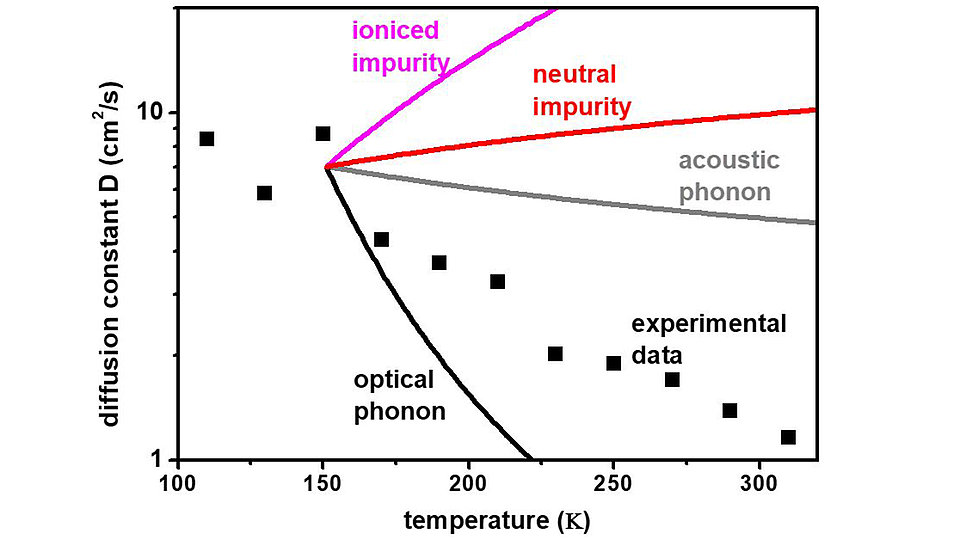
To evaluate charge carrier diffusivity, InGaN sensor layers beneath GaN cap layers of varying thickness were utilized. The PL intensity of the sensor layers decreases when charge carriers, initially excited in the cap, have to diffuse through a thicker top GaN layer. Such an experiment permits the determination of diffusion lengths in GaN. The deduced temperature-dependent diffusion coefficients showed that charge carrier diffusion in GaN is limited by phonon scattering at device operation temperatures and hole diffusion cannot be significantly improved by MOVPE growth optimization. These and other analytical methods are offered by FBH’s materials analytics group to support the epitaxial growth of III-V semiconductors and to provide information about direct band gap semiconductors.
Publications
[1] C. Netzel, V. Hoffmann, S. Einfeldt, and M. Weyers, “Optimization of the Epitaxial Growth of Undoped GaN Waveguides in GaN-Based Laser Diodes Evaluated by Photoluminescence”, J. Electron. Mater., vol. 49, no. 9, pp. 5138-5143 (2020).
[2] C. Netzel, V. Hoffmann, J. W. Tomm, F. Mahler, S. Einfeldt, and M. Weyers, “Temperature-Dependent Charge Carrier Diffusion in [0001] Direction of GaN Determined by Luminescence Evaluation of Buried InGaN Quantum Wells”, phys. stat. sol. (b), vol. 257, no. 6, pp. 2000016 (2020).


