Lateral rutile germanium dioxide MOSFET devices for next-generation high-voltage applications
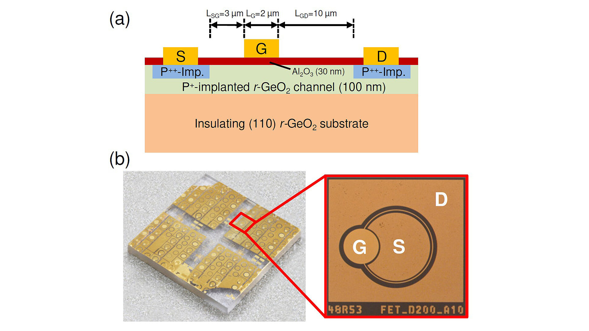
Fig. 1. Schematic cross section of the fabricated r-GeO2 MOSFET devices (a) and as well as a fully processed 5 × 5 mm² r-GeO2 wafer with a magnified image of a circular field-effect transistor (b).
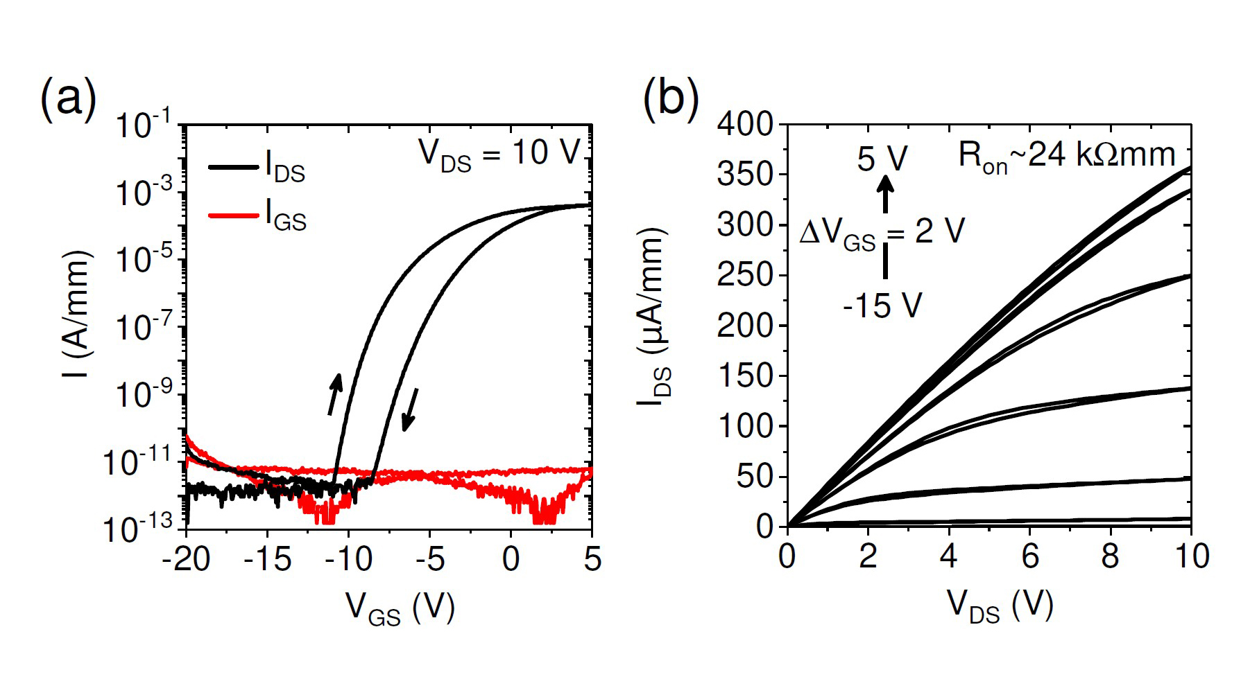
Fig. 2. Transfer (a) and output characteristics (b) of the fabricated circular r-GeO2 transistor devices.
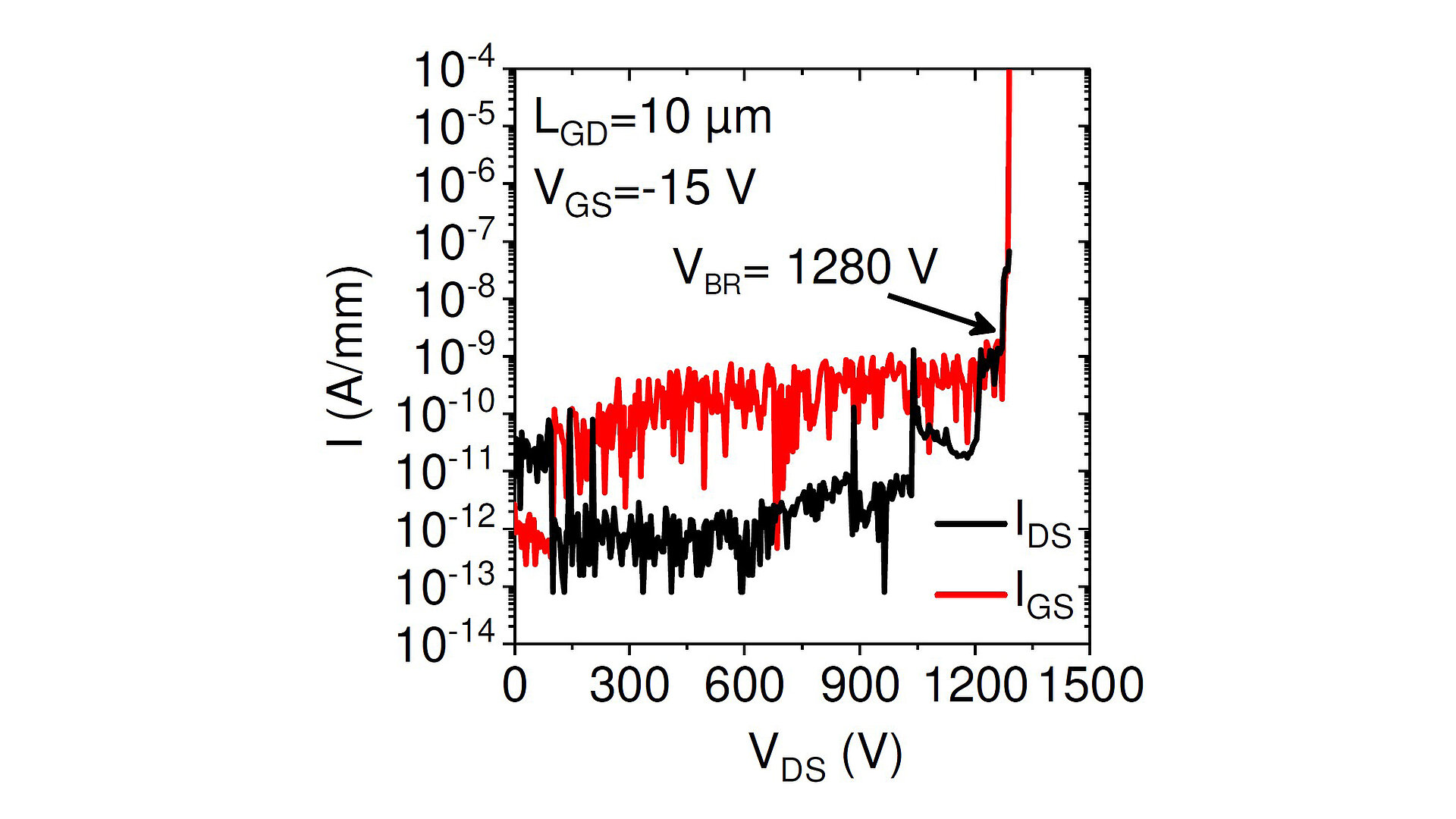
Fig. 3. Three-terminal off-state breakdown measurement of a circular r-GeO2 transistor with a gate-to-drain separation of 10 µm showing catastrophic breakdown at 1280 V.
Ultra-wide bandgap (UWBG) semiconductors such as Ga2O3, diamond, and AlN are advancing power electronics by enabling higher breakdown voltages, lower losses, and improved high-temperature operation compared to Si, SiC, and GaN. Rutile germanium dioxide (r-GeO2) has recently emerged as a particularly promising contender. It combines an ultra-wide bandgap of (4.7-5.6 eV) with a theoretically predicted critical electric field exceeding 6 MV/cm. Together with its relatively low electron effective mass and estimated room-temperature mobility around 300 cm2/Vs, r-GeO2 offers an attractive trade-off between high-voltage blocking capability and low on-state resistances.
Beyond its electronic properties, r-GeO2 can be grown as high-quality bulk single crystals at comparatively low temperatures. This reduces cost and enables the use of conducting and insulating native substrates for device fabrication. It also exhibits significantly higher thermal conductivity than β-Ga2O3, facilitating more efficient heat removal under high-power operation. More importantly, both n-type and p-type conductivity appear feasible, opening the door to true p-n junctions and bipolar devices – a major challenge for many UWBG materials.
In collaboration with the Leibniz-Institut für Kristallzüchtung (IKZ), FBH has recently started the development of r-GeO2-based power transistors for high-voltage applications. The experiments were carried out on 5 × 5 mm² insulating r-GeO2 substrates prepared from single crystals grown at IKZ. In order to realize the Ohmic contact and channel regions, phosphorous ion implantation and activation was carried out to achieve n-type conductivity. The subsequent fabrication process sequence involved atomic layer deposition of the Al2O3 gate oxide and Ti/Au-based gate and Ohmic contacts. The device structure of the r-GeO2 transistor as well as a fully processed r-GeO2 wafer featuring circular transistors are presented in Fig. 1.
Representative transfer and output characteristics of a r-GeO2 transistor device are shown in Fig. 2. The transfer characteristics show excellent current modulation with on/off ratios >108. The output characteristics show a linear current-voltage curve without any signs of increased ohmic contact resistance. In addition, a maximum drain current of 350 μA/mm was measured. Furthermore, three-terminal off-state breakdown measurements were carried out at VGS = ‑15 V. As can be seen in Fig. 3, gate and drain leakage currents stayed below 10-9 A/mm until catastrophic breakdown occurred at 1280 V, leading to irreversible destruction to the device. This value corresponds to an average drift-zone breakdown field of around 1.3 MV/cm.
These results demonstrate the first functional r-GeO2-based transistor fabricated on single-crystal insulating r-GeO2 substrates. They emphasize the high potential of this material for next-generation power electronics. Further optimization of the process technology is expected to significantly enhance device performance.
This work was funded by the Leibniz-Gemeinschaft (Senatsausschuss Wettbewerb–SAW, Germany) project under grant no. K417/2021.
Publication
[1] K. Tetzner, Z. Galazka, A. Thies, A. Külberg, O. Hilt, "Lateral rutile GeO2 MOSFET devices on single-crystal r-GeO2 substrates," in IEEE Electron Device Letters (2026).