Filling the gap – potential shifting driver amplifier suited to complete digital GaN-based signal chains
Transistors operated in switching mode (only in on- or off-state) are becoming more and more the core elements in latest circuits for applications like power electronics or efficient microwave power amplification. Here, GaN technology offers solutions also at high switching speeds. For example, GaN-based high frequency DC/DC converters with monolithically integrated active components as well as the fully digital transmitter architecture for the future mobile infrastructure are extending the present limits of system performance. However, all the circuits are facing the same challenge: to properly drive the GaN-HEMTs.
In each of these systems a digital signal source like a modulator generates the pulse sequences for the digitally driven transistors. But these sources are commonly realized in highly integrated logics with low breakdown voltages like provided by SiGe or BiCMOS and offer maximum 2 Vpp output swing. As GaN-HEMTs typically require an input voltage swing of 5 Vpp to completely switch on (Vgs = +1 V) and off (Vgs = -4 V) a power (pre-) amplifier between signal source and GaN input is required. Moreover, DC-coupled, digital multi-stage GaN power amplifiers need an adjustable DC potential shift when driven with different broadband input modulation schemes.
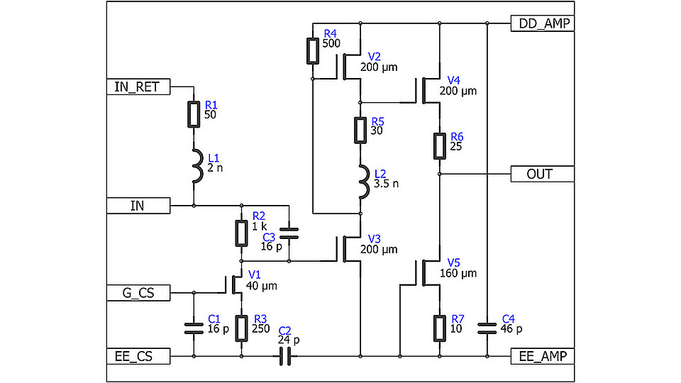
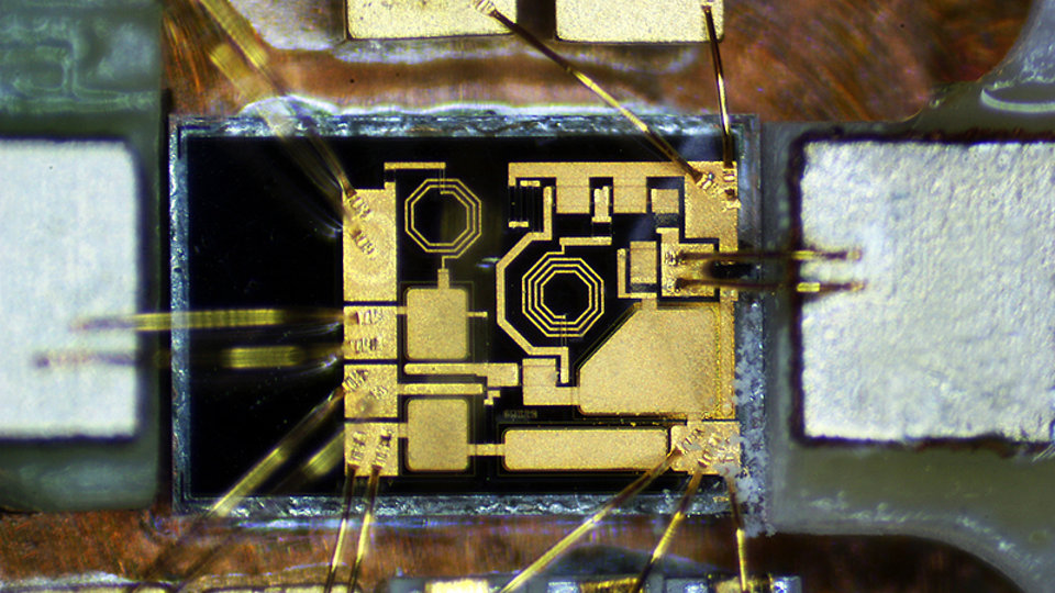
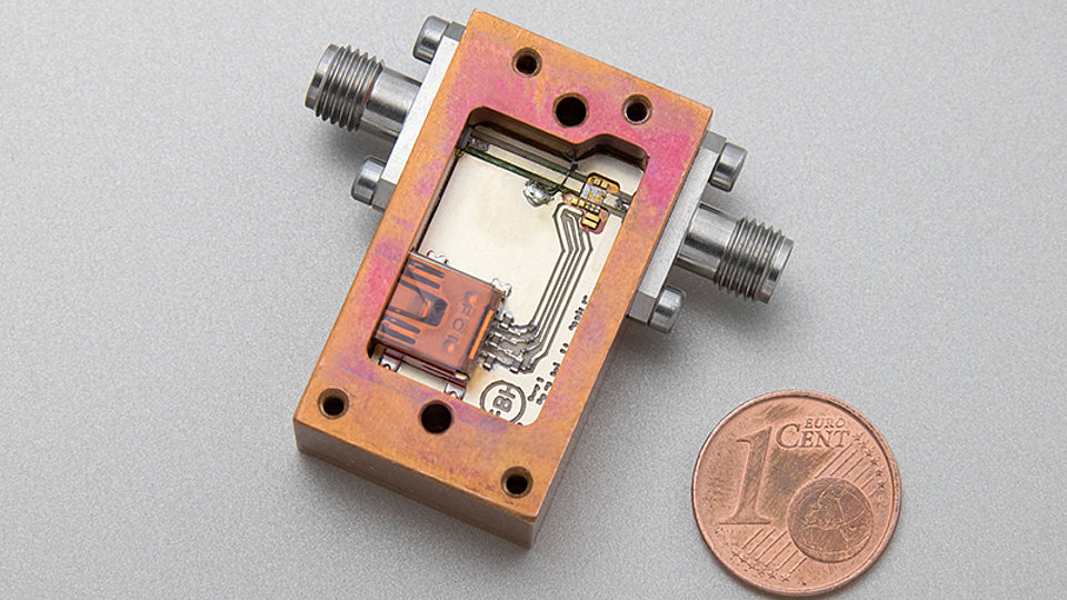
In August 2020, FBH has presented a GaN-based driver amplifier (PSA) module with included DC potential shifting at the virtual International Microwave Symposium 2020. The module is suitable for properly driving GaN-HEMTs with digital bit sequences in the microwave range. With it, a GaN-HEMT can be driven with 5 Vpp input swing from a standard 1 Vpp signal. Additionally, the PSA provides a controllable potential shift (DC-offset) between -1.5 V to -10.9 V when referenced to ground. A voltage gain of 10.7 and 4.9 with a load of 1 kΩ || 0.25 pF and 50 Ω is achieved, respectively. Input of the PSA is referred to GND with 50 Ω input impedance. The bandwidth is DC - 3.2 GHz for a 3 dB voltage gain drop for both loads applied. Overall power consumption is 2.3 W. The proposed PSA is an important part to complete digital signal chains and can be also used as analog amplifier. It bridges the gap between high-speed digital signal sources and the digital GaN part. Together with control electronics it has been realized as a compact module
This work was supported by the German Federal Ministry of Education and Research (BMBF) within the “Research Fab Microelectronics Germany (FMD)” framework under ref. 16FMD02.
Publication
[1] T. Hoffmann, F. Hühn, S. Shevchenko, W. Heinrich and A. Wentzel, "Broadband Driver Amplifier with Voltage Offset for GaN-based Switching PAs", 2020 IEEE/MTT-S International Microwave Symposium (IMS), Los Angeles, CA, USA, 2020, pp. 273-276, doi: 10.1109/IMS30576.2020.9223837.


