Digitizing 6G – sub-THz switch-mode circuits for highly efficient wireless communication systems
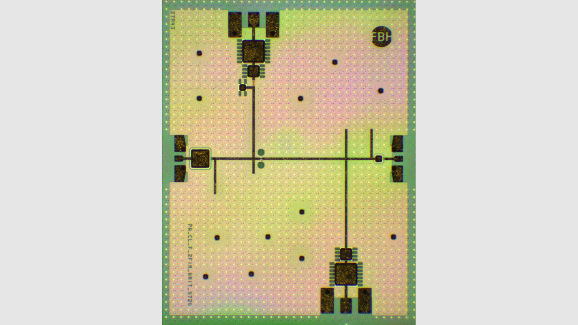
Fig. 1. Chip photo of a fabricated InP class-F-like W-band PA; area: 1.3 x 1.6 mm2.
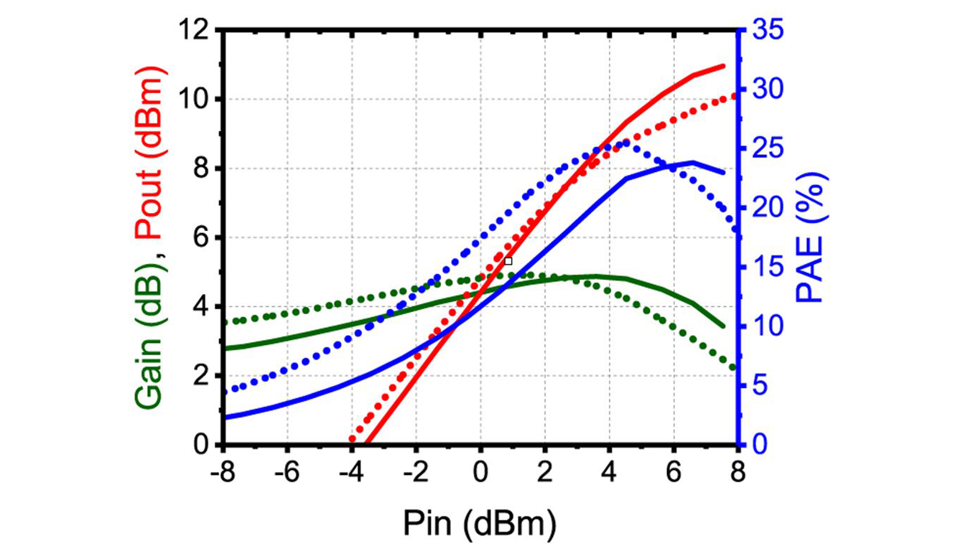
Fig. 2. Measured Pout, large-signal gain and PAE vs. Pin; bias1: Vcc = 2.9 V, Vb = 0.9 V (solid lines), bias2: Vcc = 2.85 V, Vb = 0.87 V (dotted lines).
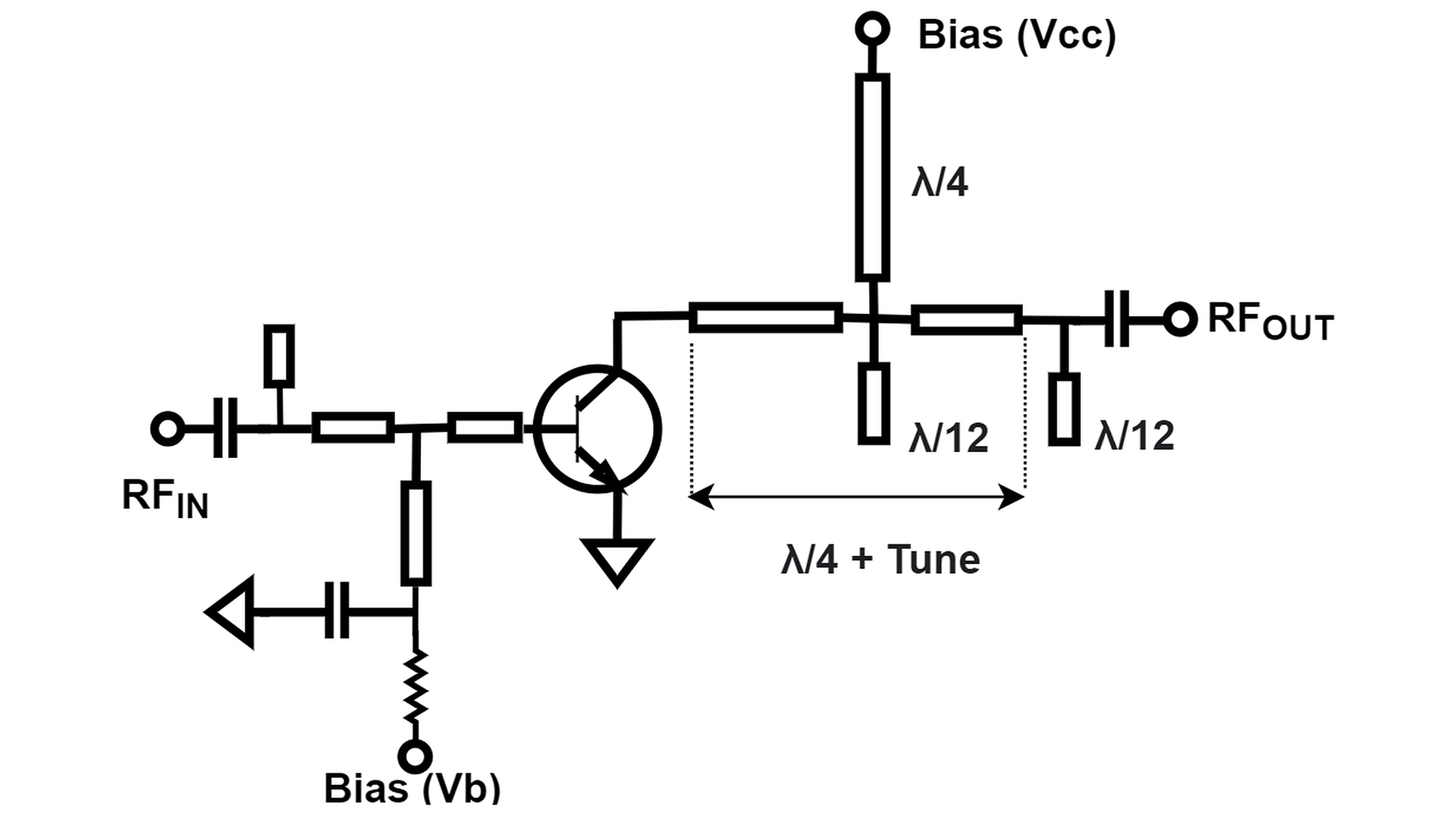
Fig 3. Schematic of class-F like 100 GHz power amplifier.
The W-band spectrum (75 … 110 GHz) is gaining more and more attention. This is especially true for commercial, military and 6G applications that require wireless data transmission with high capacity and low-cost at the same time. The top priority for such systems is high output power, gain and bandwidth as well as proof-of-MIMO system operation and functionality with multi-element arrays at highest frequencies. However, the power-added efficiency (PAE) of the power amplifiers (PAs) is still a bottleneck. The PA is a major power dissipation contributor in the front-end, thus significantly affecting the overall efficiency.
Among different approaches for efficiency enhancement in PAs at mm-waves, switched-mode concepts like class-E/F seem to be the most promising solution for W-band and beyond. However, it is a major challenge to fine-tune class-E/F networks for W-band. This can be attributed to significant parasitics and degrading accuracy of the models at the harmonics involved. Another important factor is proper modelling of the high current regime in the transistor’s saturation region. At the same time, InP technology is the most promising candidate for both high efficiency and high output power requirements at W-band. It is therefore highly interesting to evaluate the potential of switch-mode W-band PA designs in terms of efficiency using FBH 0.5 μm InP-DHBT process line for the application in next-generation (6G) communication systems.
In 2021, we have presented the first single-stage class-F-like W-band power amplifier in InP-DHBT technology. The compact chip (1.3 x 1.6 mm2) reaches a maximum efficiency of 25.4 % at 8.8 dBm output power for a collector voltage VCC of 2.85 V and a base bias (Vb) of 0.87 V. However, the best trade-off between Pout (10.9 dBm) and PAE (24 %) has been achieved for a slightly different bias point (VCC = 2.9 V and Vb = 0.9 V). The measured saturated output power is 12.5 dBm. The proposed PA was also measured with several biasing conditions over a wider frequency range from 92 to 103 GHz with peak PAE between 23 and 25 %, Pout between 9 and 12 dBm and 4 – 5 dB gain.
This PA achieved state-of-the-art results for InP-based switch-mode configurations around 100 GHz. Above 100 GHz, it reached the highest PAE so far. The performance obtained is promising and serves as a good starting point to develop further highly efficient switch-mode PA designs. These designs are supposed to significantly improve energy efficiency in future high-speed communication systems and will thus push the digitization of 6G.
This work was funded by the German Research Foundation (DFG) under ref. WE 6288/2-1. It was additionally supported by the German Federal Ministry of Education and Research (BMBF) within the “Research Fab Microelectronics Germany (FMD)” framework under ref. 16FMD02.
Publication
A. Shrestha, R. Doerner, H. Yacoub, T.K. Johansen, W. Heinrich, V. Krozer, M. Rudolph, A. Wentzel, “A 100 GHz Class-F-Like InP-DHBT PA with 25.4 % PAE“, accepted for publication in Proceedings of the 16th European Microwave Integrated Conference (EuMiC) London, UK (2021).