Traceability for electrical measurements at millimeter-wave and terahertz frequencies
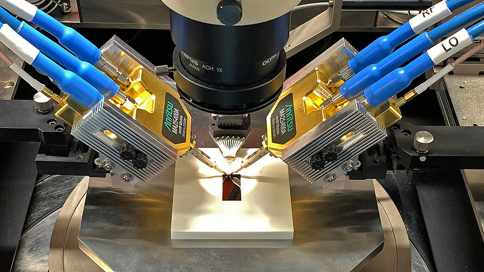
Fig. 1: On-wafer probing of calibration standards. On the left and the right side, the probes, the probe holders and the cables connecting the probes to the network analyzer are visible. The microscope on top is employed to carefully position the probe holders.
Future generations of wireless systems will operate in the 100 GHz to 1 THz frequency range. These systems will enable a large variety of applications such as radar sensing and imaging, high-capacity communications, and high-accuracy positioning. Therefore, they are expected to influence the future of our digitized society. Developing the electronics for these applications requires traceable electrical measurements at millimeter-wave and THz frequencies. Traceability is referring to an unbroken chain of comparisons relating measurements to a known reference.
In the framework of the European project “Traceability for Electrical Measurements at Millimetre-wave and Terahertz Frequencies for Communications and Electronics Technologies” (TEMMT) such traceability for electrical measurements at millimeter-wave and terahertz frequencies will be established. Together with well-known metrology institutes from across Europe (VSL Dutch Metrology Institute, National Physical Laboratory, Laboratoire National de Métrologie et d'Essais and Physikalisch-Technische Bundesanstalt), with universities (Chalmers University of Technology and Université de Lille), and with industry partners (Anritsu, FormFactor and Keysight), the Ferdinand-Braun-Institut is developing traceability and verification techniques for on-wafer measurements to cover frequencies from 110 GHz to 1,100 GHz.
On-wafer measurements allow to characterize the devices under test directly on the wafer, as shown in Fig. 1. These on-wafer measurements require calibration techniques in order to deduct the parasitic effects due to cables, probes and the measurement instrumentation from the true behavior of the device. To quantify these parasitic effects, well-defined reference structures on the wafer need to be measured in addition to the device under test.
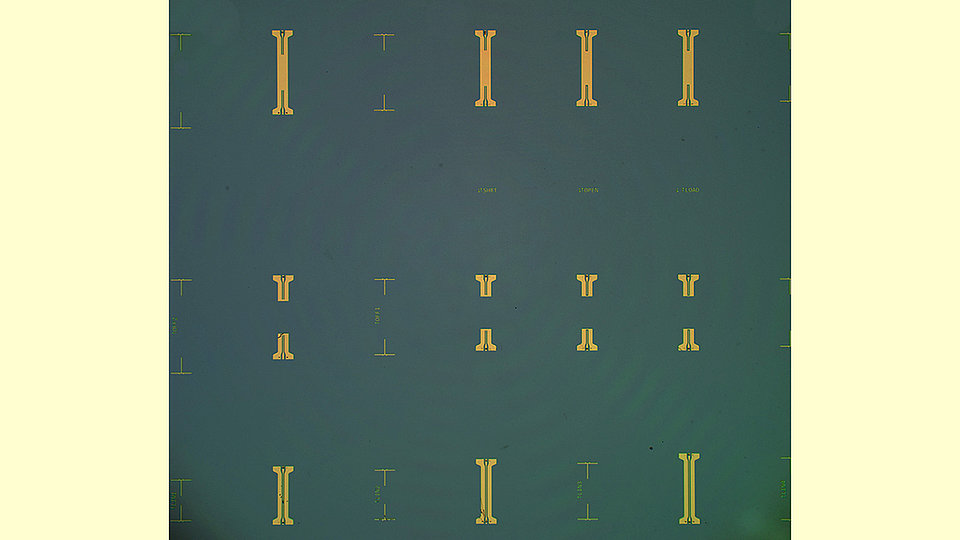
Together with its partners, FBH designed two on-wafer calibration kits with reference structures for the bands 110 GHz to 330 GHz and for 330 GHz to 1,100 GHz. They consist of lines with various lengths and various reflection stubs. Université de Lille manufactured the two calibration kits on silicon wafers and distributed them to the project partners for on-wafer characterization. Fig. 2 shows the calibration kit for the 110 GHz to 330 GHz band. At the ends of each structure, landing pads are located to probe the structure. Based on the measurements of the calibration kits, uncertainty sources will be identified and characterized and uncertainty calculations will be performed to finally obtain traceable calibration and verification measurements up to 1,100 GHz.
The TEMMT project is a EURAMET joint research project and receives funding from the Horizon 2020 European Union Funding for Research & Innovation under the European Metrology Programme for Innovation and Research (EMPIR). EMPIR is the main funding program for European research on metrology. The TEMMT project is running from May 2019 to April 2022. In total, 16 European and 3 international organizations are involved.

