GaN HEMT modeling based on Chalmers model and pulsed S-parameter measurements
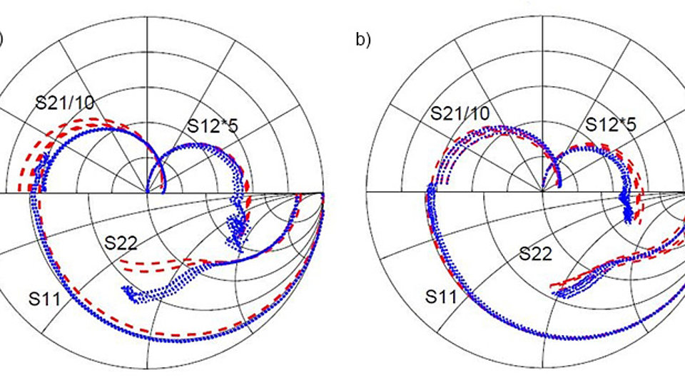
Fig. 2: S-parameters at Vds = 28 V of 2 x 125 μm GaN HEMT for a) static S-parameter up to 50 GHz and b) pulsed S-parameter up to 40 GHz
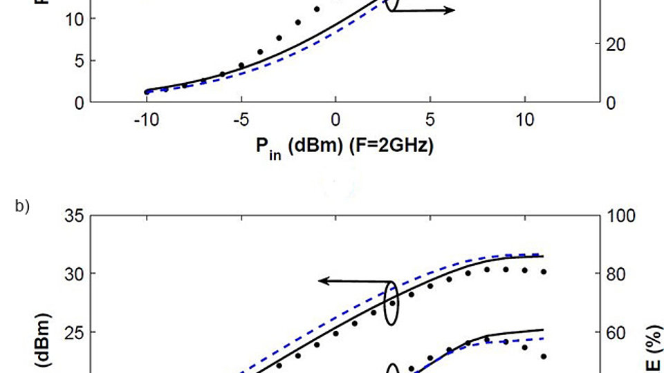
Fig. 3: Output power and power added efficiency as a function of input power with bias voltage as parameter: measurements (symbols) and simulation with model from static S-parameter measurements (blue) and simulation from pulsed S-parameter measurements (black) at a) 2 GHz and b) 8 GHz (Vds = 28 V and Ids =10 mA).
Today, GaN high electron mobility transistors (HEMTs) have demonstrated extraordinary microwave performance including high power density, high gain, and low noise. With respect to reliable computer-aided circuit design, the impact of unavoidable self-heating and uncontrollable trapping effects render it highly challenging to provide transistor models of good quality. Specifically, the widely used static measurements and standard models cannot satisfy the need of high accuracy for power characterization in the modeling process. Thus, our approach is to rely on a conventional model but to extract the model parameters through pulsed S-parameter measurement.
The major advantages of modeling with pulsed S-parameter measurements is that the measurements can be seen as iso-thermal measurements. The modeled trap state can be the same as in an actual transistor operation, when a commonly used DC supply voltage is utilized as quiescent bias point. It can therefore be expected to model GaN HEMT devices with dispersion using Chalmers model, which lacks concrete trap descriptions.
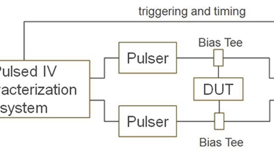
The experimental setup for the pulsed measurements is shown in Fig. 1. The pulsed measurement system is supplied with two external pulser heads, which provide a variety of pulsed voltage and current ranges and different pulse lengths. In this measurement, the pulse bias length is 250 ns and the duty cycle of pulse is 0.1%; they were kept short enough so that the self-heating effect will not affect the device characteristics. On the other hand, the system is also supplied with four external power supplies, which provide the quiescent and non-quiescent voltages for both gate and drain. In this measurement, Vgs = -2.3 V and Vds = 28 V were used as quiescent bias points, because they are commonly used bias points in our applications so that we can get a trap state, which is identical with the certain applications.
The parameter extraction routine is based on multi-bias S-parameter measurements, where the drain voltage is swept from 0 V, and the gate voltage is swept from below pinch-off to +1 V. In addition, cold field-effect transistor measurements are performed in order to determine the extrinsic elements. For all measured S-parameters, small-signal equivalent-circuits are determined. The parameters of the Chalmers models charge functions are then determined by fitting the large-signal models capacitances to the small-signal equivalent-circuit parameters. In case of the drain current Ids, the model can be directly fitted against the currents that were measured along the S-parameter measurements.
The comparison of measured and modeled S-parameters at Vds = 28 V for the two models based on static and pulsed measurement is shown in Figs. 2a and 2b, respectively. As can be seen, a better agreement in the S-parameters, particularly S21, has been achieved with the model based on pulsed S-parameter measurements.
Fig. 3 shows the comparison between the simulation results of extracted models from the standard and pulsed S-parameter measurements. It demonstrates that the output power Pout in linear region at both frequencies is described by the simulation with model base on pulsed measurements with better accuracy. Thus, it can be concluded that Chalmers model is able to describe the transistor performance, if the model is determined relying on pulsed S-parameters, where the quiescent bias point should be restricted to a fixed bias point. The sophisticated measurement and parameter extraction procedure thereby enables the use of standard circuit simulator models even for GaN HEMT devices that are subject to trapping effects.
Publications:
P. Luo, O. Bengtsson, M. Rudolph, “Reliable GaN HEMT Modeling Based on Chalmers Model and Pulsed S-Parameter Measurements”, German Microwave Conference (GeMIC), 2016.
P. Luo, O. Bengtsson, M. Rudolph, “Novel Approach to Trapping Effect Modeling based on Chalmers Model and Pulsed S-Parameter Measurements”, European Microwave Integrated Circuits Conference (EuMIC), 2016.


