Electromagnetic Field Simulations to Improve Understanding of Parasitic Effects of On-Wafer Scattering Parameter Calibrations
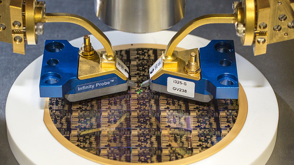
Fig. 1: Setup of an on-wafer scattering parameter measurement. The wafer is placed on a dielectric chuck (white cylinder below the wafer).
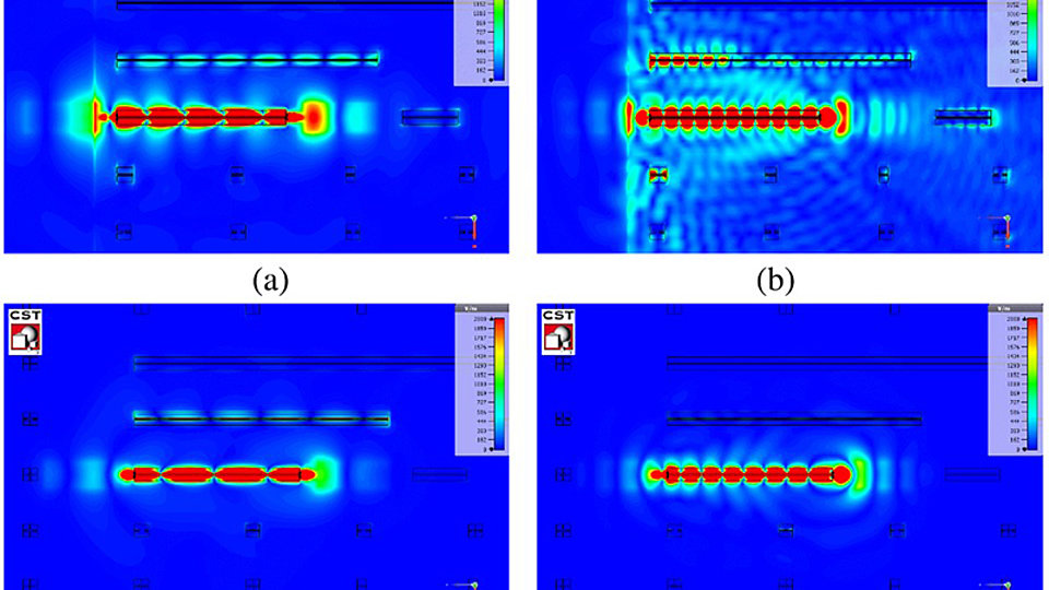
Fig. 2: Simulation of electromagnetic fields on coplanar waveguides built on different substrates. Plots show the magnitude of the electric field: (a) Al2O3 substrate at 40 GHz, (b) Al2O3 substrate at 100 GHz, (c) SiO2 substrate at 40 GHz, (d) SiO2 substrate at 100 GHz.
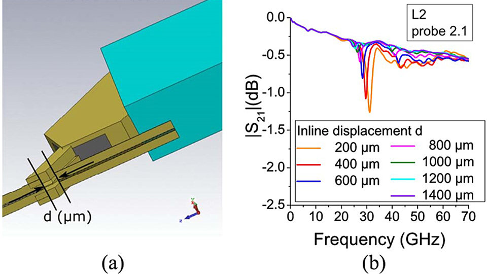
Fig. 3: (a) Computer model of a probe landed on a coplanar waveguide (substrate is hidden for clarity). Another coplanar waveguide is located below the prober and acts as perturbation of the setup. (b) Calibrated absolute transmission of the excited coplanar waveguide dependent on the distance d. Small distances d lead to large perturbations and to parasitic dips in the calibrated transmission of the coplanar waveguide.
On-wafer measurements of S-parameters are required to directly characterize devices under test (DUTs) on the wafer. The DUTs are, e.g., individual components such as transistors, filters or complete circuits, which can be used for wireless communications, automotive radar, and medical sensing. Calibration approaches such as mTRL are employed to account for systematic measurement errors. The measurement of on-wafer calibration standards in addition to the raw S-parameters of the DUT allows for characterizing these errors and for obtaining the S-parameters of the DUT itself. Fig. 1 depicts the setup of an on-wafer scattering parameter measurement using one of FBH’s prober stations. The wafer is located on a dielectric chuck, and probes are used to contact the respective DUT on the wafer. The probes are equipped with needles connecting the DUT to the vector network analyzer (not shown in the figure). The probes can be adjusted with the help of a microscope (silver cylinder at the top of figure) using stepper motors.
In a framework of joint projects with various metrology institutes and partners from across Europe, FBH’s Microwave Department models on-wafer S-parameter measurements using 3D electromagnetic field simulations to understand the occurring parasitic effects. Numerical modeling is an appealing tool for these investigations due to the absence of uncertainties such as in the shape of the geometries and in the respective material parameters. Furthermore, numerical simulations deliver field plots which provide descriptive insight into the measurement process. A further crucial advantage of electromagnetic simulations is the ability to run systematic perturbation studies to estimate the influence of geometry and material parameters on the quality of the calibration.
The performed simulations show that even for a configuration without neighboring structures on the wafer, the calibration algorithm is not capable of completely compensating the probe influences. Therefore, small deviations of the calibrated S-parameters remain. The calibration may become worse if neighboring structures are present as shown in Fig. 2. The figures depict the simulated absolute value of electric fields resulting from the excitation of a coplanar waveguide with probes. The electric fields are shown for two substrates: (a) and (b) Al2O3 with the relative permittivity εr = 9.7 and (c) and (d) SiO2 with the relative permittivity εr = 3.78. For all simulations, the wafer is placed on a ceramic chuck with εr = 6.5. Fig. 2 (a) and (c) show an excitation at 40 GHz and (b) and (d) an excitation at 100 GHz. The parasitic coupling of fields to neighboring structures is much stronger on the Al2O3 wafer than on the SiO2 wafer. This may lead to a poor quality of the calibrated S-parameters. Further systematic studies revealed that the parasitic coupling can be suppressed if, e.g., the dielectric constant of the chuck material is similar to or larger than the dielectric constant of the substrate.
Fig. 3 depicts a parameter study investigating the influence of a perturbing neighboring coplanar waveguide on the quality of the calibrated scattering parameters. Fig. 3 (a) presents a probe touching a coplanar waveguide. The perturbing waveguide is placed in line with the distance d. Resonances of the neighboring waveguide appear as dips dependent on d in the S-parameters of the DUT after calibration as shown in Fig. 3 (b). The strength of these effects is governed by the dimensions of the probes and by the distance between the probes and the perturbing structures. Further simulations show that the effective area on the lower side of the probe, which is referred to as probe shadow, is crucial. The probe shadow should be kept free of structures to avoid parasitic probe coupling and poor S-parameter calibrations.
The design guidelines resulting from these investigations were provided to the scientific community through publications and recent conference contributions.
Acknowledgement
This work was supported in part by the European Metrology Program for Innovation and Research (EMPIR) through the Microwave Measurement for Planar Circuits and Components Project under Grant 14IND02 (funding period: 01.10.2015 – 01.10.2018). The EMPIR program is co-financed by the participating countries and from the European Union’s Horizon 2020 research and innovation program.
Publications
[1] U. Arz, K. Kuhlmann, T. Dziomba, G. Hechtfischer, G. N. Phung, F. J. Schmückle, W. Heinrich, “Traceable Coplanar Waveguide Calibrations on Fused Silica Substrates up to 110 GHz”, in IEEE Transactions on Microwave Theory and Techniques, vol. 67, no. 6, pp. 2423-2432, June 2019, doi: 10.1109/TMTT.2019.2908857
[2] G. N. Phung, F. J. Schmückle. R. Doerner, B. Kähne, T. Fritzsch, U. Arz, W. Heinrich, “Influence of Microwave Probes on Calibrated On-Wafer Measurements”, in IEEE Transactions on Microwave Theory and Techniques, vol. 67, no. 5, pp. 1892-1900, May 2019, doi: 10.1109/TMTT.2019.2903400
[3] G. N. Phung, F. J. Schmückle, R. Doerner, W. Heinrich, T. Probst, U. Arz, “Impact of Substrate Modes on mTRL-Calibrated CPW Measurements in G Band”, in Proc. 48th European Microwave Conference (EuMC), Madrid, 2018, pp. 194-197, doi: 10.23919/EuMC.2018.8541813


