Basis for improved UV LEDs – high-quality aluminum nitride by high-temperature annealing
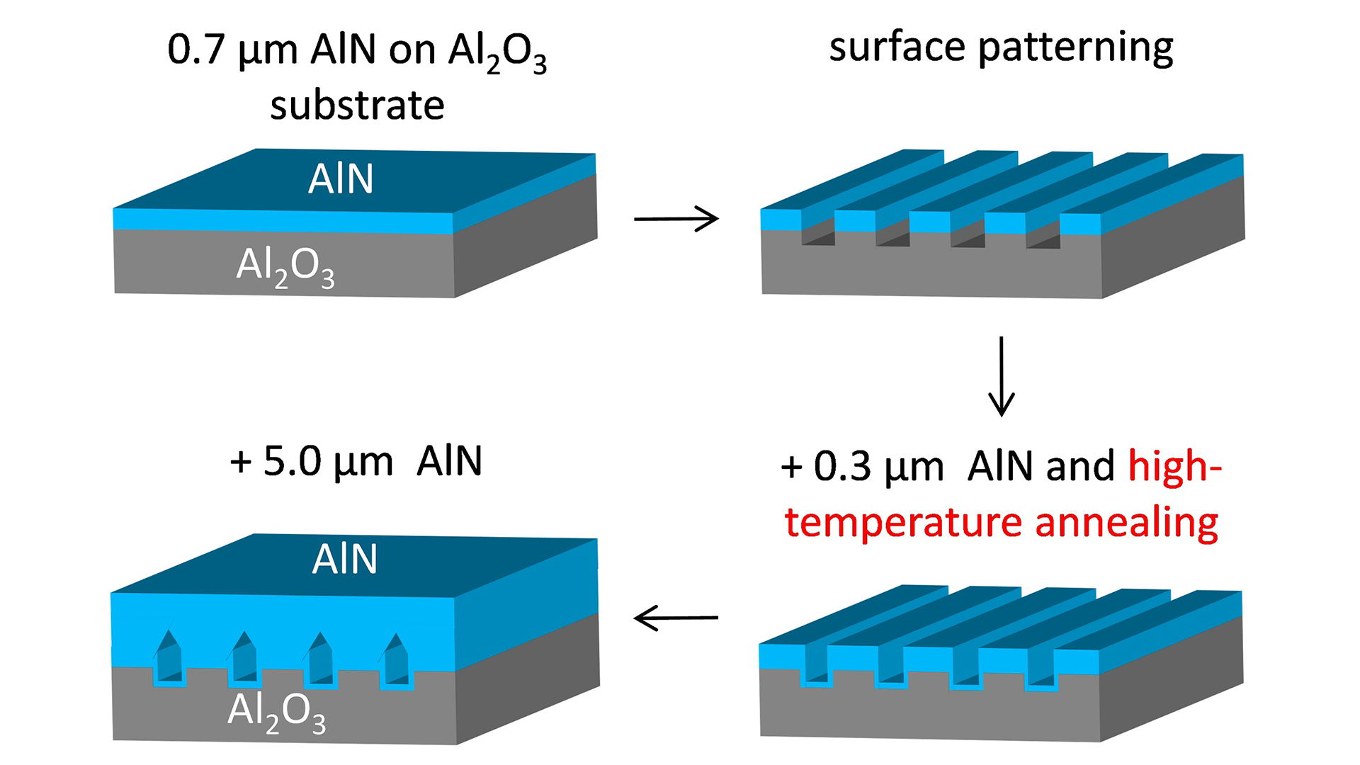
Fig. 1: Process chain to combine a patterned AlN/Al2O3 interface and high-temperature annealed AlN.
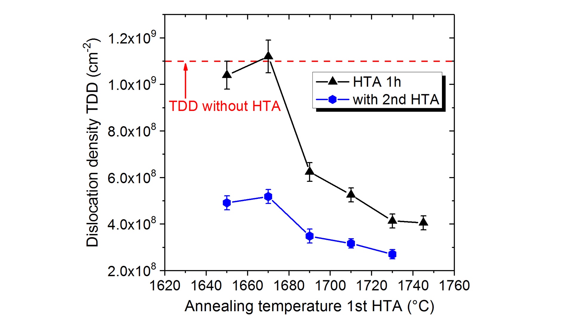
Fig. 2: The TDD in the AlN layer decreases with increasing annealing temperature. A second annealing further reduces the TDD.
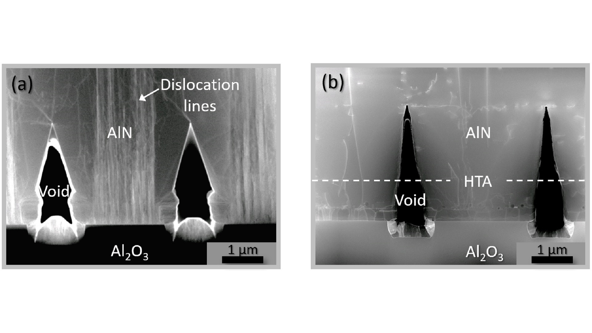
Fig. 3: Cross-section transmission electron microscopy images showing how effectively propagation of dislocation lines above the trenches (a) can be avoided by an intermediate HTA step (indicated by dashed line) (b).
Ultraviolet (UV) light emitting diodes (LEDs) can be utilized in several fields of applications including medicine, production, disinfection, environment, and life sciences. Very recently, using UV LEDs to kill the COVID-19 virus attracted public interest.
To constantly improve the performance of such UV LEDs, the material that provides the basis for these devices must be continuously optimized. Commonly, crystalline substrates are used to manufacture UV LEDs. In this context, it is necessary to epitaxially grow an aluminum nitride (AlN) layer with a smooth surface as defect-free as possible on commercially available sapphire (Al2O3) substrates.
To improve the material quality of the AlN layer, a high-temperature annealing (HTA) process at up to 1745 °C has recently been established at FBH. For increased light extraction from the UV LEDs, a patterned AlN/Al2O3 interface is preferred to guide the light out of the LED chip. Therefore, the combination of our well-established lithography-based interface patterning and HTA to further improve the AlN material quality was investigated.
The preparation sequence shown in Fig. 1 turned out to be the most promising solution to combine these processes. Firstly, the AlN/Al2O3 substrate with plane interface is patterned into ridges of 2 µm width, separated by 1.5 µm wide and 1.2 µm deep trenches. Secondly, the uncovered Al2O3 trench walls are covered by 0.3 µm AlN to better protect the pattern during the following high-temperature treatment.
The patterned surface is then fully overgrown with 5.0 µm AlN until full coalescence above the trenches and an overall smooth surface are reached. The temperature during the one-hour annealing process decisively determines the material quality, in particular the threading dislocation density (TDD). Threading dislocations reduce the UV radiation generated within the LED, negatively affect the electrical device properties, and shorten the LED life time.
Our experiments show that with increasing annealing temperature, a decrease of the TDD from 11 × 108 cm-2 to 4 × 108 cm-2 can be reached (Fig. 2). Furthermore, applying a second HTA to the fully grown AlN layer at the end of the process chain (Fig. 1) further reduces the TDD (Fig. 2). TEM images in Fig. 3 reveal how effectively the number of dislocations is reduced by a single annealing step at 1730 °C. They directly compare AlN layers without and with HTA treatment.
With these improvements, the efficiency of UVC LEDs emitting at 265 nm was increased by a factor of 1.4, and an extrapolated device lifetime of more than 10000 hours was achieved.
This work was partially supported by the German Federal Ministry of Education and Research (BMBF) through the consortium “Advanced UV for Life” under the project contracts 03ZZ0130A, and 03ZZ0134B.
Publications
S. Hagedorn, S. Walde, A. Knauer, N. Susilo, D. Pacak, L. Cancellara, C. Netzel, A. Mogilatenko, C. Hartmann, T. Wernicke, M. Kneissl, M. Weyers, "Status and Prospects of AlN Templates on Sapphire for Ultraviolet Light-Emitting Diodes", Phys. Status Solidi 217, 1901022 (2020).
S. Hagedorn, A. Mogilatenko, S. Walde, D. Pacak, J. Weinrich, C. Hartmann, M. Weyers, "High-Temperature Annealing and Patterned AlN/Sapphire Interfaces", Phys. Status Solidi B 258, 2100187 (2021).