Advances in Physical Simulation of Transferred Substrate InP/InGaAs DHBT
Recent advances in physical device modeling of our in-house transferred substrate InP/InGaAs double heterostructure transistors for THz applications are leading to refined device models. Device modeling is crucial for circuit design as well as understanding and solving possible shortcomings in the device design and the fabrication process.
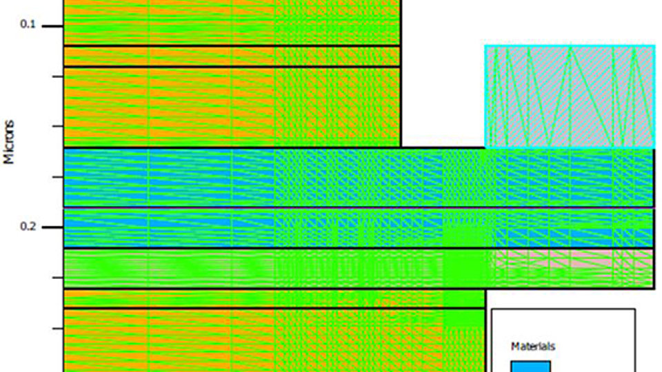
To "calibrate" device simulation, which is based on the basic semiconductor equations governing the electron transport through the structure, several material constants need to be adjusted. To achieve this, we have implemented the epitaxial structure and the doping profile in the Silvaco simulation framework with an adequate mesh grid of 6000 points, including refinement on the E-field, electron temperature, and recombination rate. The built-in velocity models, originally optimized for Silicon, were calibrated with experimental data obtained from S-parameter measurements. Two complementary models were used for the electron velocity. The first is a low field mobility, which is depending on concentration, composition, and temperature. The second model is embedded within Silvaco ATLAS and employs a field-dependent mobility. In both cases, the values of the critical fields and velocity saturation were tuned to fit the InP and InGaAs compounds. The proper modeling of the base p-InGaAs layer is critical for fmax and gain performance. Due to its heavy doping and reduced thickness, strong recombination occurs in the base region. The recombination is dominated by Auger and Shockley-Read-Hall mechanisms.
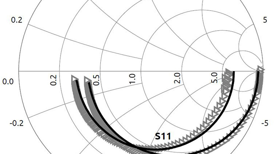
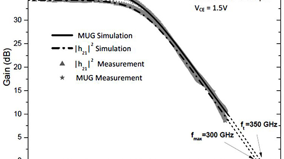
Carrier concentrations were calculated using the Fermi Dirac statistics and Bandgap narrowing. The energy balance model enables non-local effects such as velocity overshoot, and the dependence of impact ionization rates on carrier energy distribution. An advanced model for electron and hole relaxation time which depends on electron temperature was included. The DC characteristics show a deviation in ideality factor at low bias for the E-B junction compared to the measurements. This can be attributed to not fully accurate Auger/SRH coefficients and possibly additional recombination at the device surface in the transferred substrate HBT geometry. We used RF measurement data from 50 MHz - 110 GHz with hundreds of data points to calibrate the simulation. Excellent agreement in the small signal characteristics between the experimental data and the simulation could be achieved for frequencies up to 90 GHz. The deviation at higher frequencies can be explained by parasitic effects not included in the simulation, such as dielectric loss in the BCB or an incomplete de-embedding procedure. In conclusion, an accurate physical device model of our InP transferred substrate HBTs was simulated by proper material constant calibration.
Support from the European Commission under FP7 Marie-Curie CIG action "THzPowerElectronics" and Leibniz project "Electronic high performance components for applications between 500 and 1000 GHz" is greatly appreciated.
Publication
M. Brahem, D. Stoppel, N. Weimann, "Physical Simulation of Transferred Substrate InP/InGaAs DHBT", Proc. Compound Semiconductor Week (CSW), 14-18 May 2017, Berlin, Germany.


