A Drain-Lag Model for GaN HEMTs based on Chalmers Model and Pulsed S-Parameter Measurements
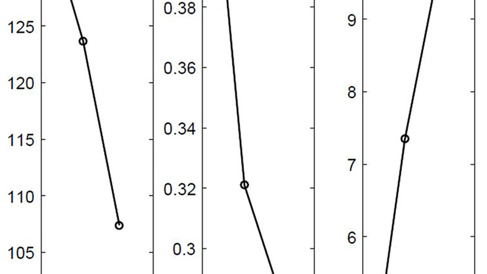
Fig. 1: Extracted values of the Chalmers model parameters depending on pulse quiescent drain voltages QVDS
GaN HEMTs are widely used these days thanks to their excellent microwave performance with regard to high power and low noise. However, modeling their trapping effects still remains a key issue. Since these effects hamper the achievable output power and linearity, much effort has been devoted to measure, understand and describe them in the last years. However, recent dedicated trap models are still not standard in commercial circuit simulators. Our approach allows us to derive an optimized set of parameters, which are sensitive to trap states, enabling optimum large-signal simulation accuracy for standard models by reproducing the trap states from the bias condition.
Recently, a new custom model was implemented that allows for dynamic simulation of trapping states in circuit simulation. Relying on an identical set of parameters in both approaches keeps the interface to the circuit designers consistent. In the following, the dynamic model is introduced, it is discussed to which extend the original approximation based on a standard model compromises accuracy in the highly nonlinear performance. For this purpose, we employed the Chalmers (Angelov) model. The model parameter extraction routine is based on pulsed S-Parameter measurements for different pulse quiescent drain voltages QVDS = 8, 15, and 28 V. The parameters of the Chalmers model’s Ids description and the charge function are then determined by fitting the IV curves to the measured pulsed IV characteristics. In this way, for each pulsed S-parameter measurement a set of model parameters is determined. It has been found that only three parameters have to be adjusted if the quiescent drain voltage varies: Ipk0, αs, and λ. The other parameters can be kept unchanged without significant loss of accuracy. Moreover, Fig. 1 reveals that these parameters show a rather linear dependence on the pulse quiescent bias point.
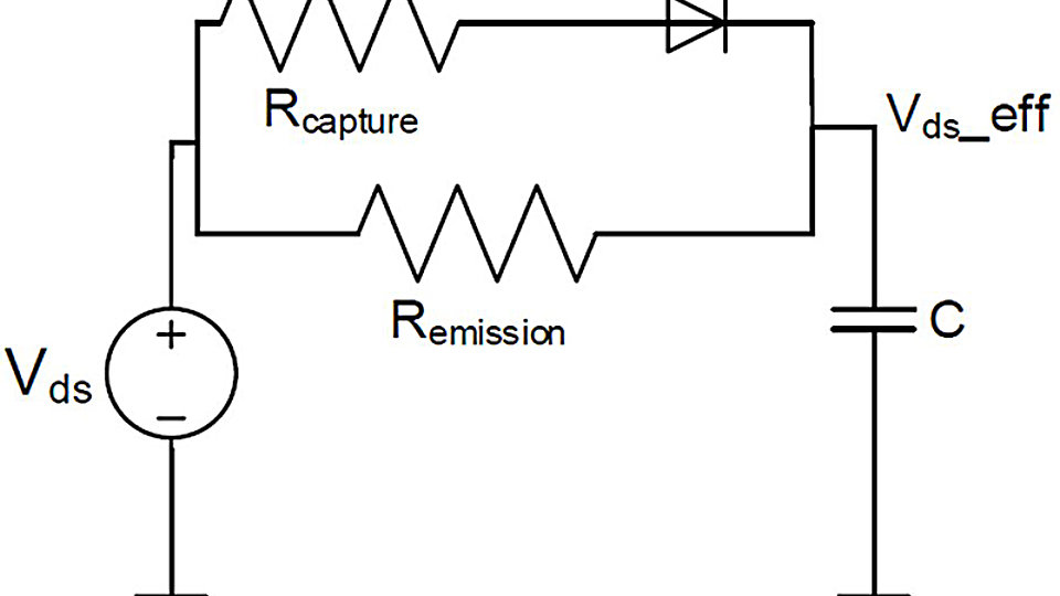
Using this dependence allows for a good prediction of the steady-state drain source currents, where the steady-state traps are controlled by input voltage vgs and output voltage vds. However, when vds is pulsed up or down, the instantaneous output current does not follow the fast vds variation but exhibits a slow current transient due to drain-lag effects. In order to take this into account we employ a subcircuit shown in Fig. 2, which is to describe the emission and capture process. When vds is pulsed from a higher voltage to a lower one, the instantaneous output current ids value first does not change and preserves the trap state related to the previous value of vds. After the discharge of capacitance C through Remission, ids gradually reaches a value depending on the trap state of the new value of vds. On the other hand, when vds is pulsed to a higher value, the response is much faster, which can be explained by a shorter time constant of the respective trapping process. With this in mind, the output voltage vds,eff of the subcircuit offers a nice solution to describe the changes in the trap states. As a result, the three voltage-dependent parameters can be defined as:
Ipk0 (vds) = Ipk0 * (1 + TrIpko* vds,eff)
αs(vds) = αs * (1 + Tralphas* vds,eff)
λ(vds) = λ *(1 + Trlambda* vds,eff)
where, TrIpk0, Tralphas, and Trlambda are new fitting parameters to adjust the drain-source current to different trap states, while vds,eff describes the emission and capture process. The time constants for these two processes are defined as:
Tcapture = Rcapture * C
Temission = Remission * C
as Remission >> Rcapture
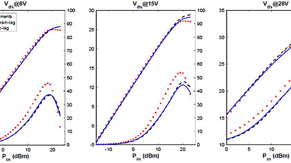
Fig. 3 presents the comparison between measured and simulated (with and without drain-lag modeling) output power and PAE, for a load condition providing maximum output power, for several Vds voltages. Measurements (symbols) are compared with simulation data of the full model including the above trap description (blue lines) and with the original Chalmers model (dashed black lines). The latter model misses the subcircuit describing the trap states dynamically, thus the model parameters were adjusted to the bias point. It is seen that the full model provides good prediction of the loadpull behavior. The standard model shows to predict the linear behavior well, but tends to over-estimate the output power, especially in the saturation region and at higher Vds condition, where the impact of drain-lag effects is more pronounced.
Publications:
P. Luo, O. Bengtsson, M. Rudolph, "Novel Approach to Trapping Effect Modeling based on Chalmers Model and Pulsed S-Parameter Measurements", in European Microwave Integrated Circuits Conference (EuMIC), London, UK, 2016.
P. Luo, O. Bengstson, M. Rudolph, "A Drain Lag Model for GaN HEMT based on Chalmers Model and Pulsed S-Parameter Measurements", in International Microwave Symposium (IMS), Honolulu, USA, 2017.


