A 26 GHz GaN-MMIC with integrated switches for discrete level supply modulation
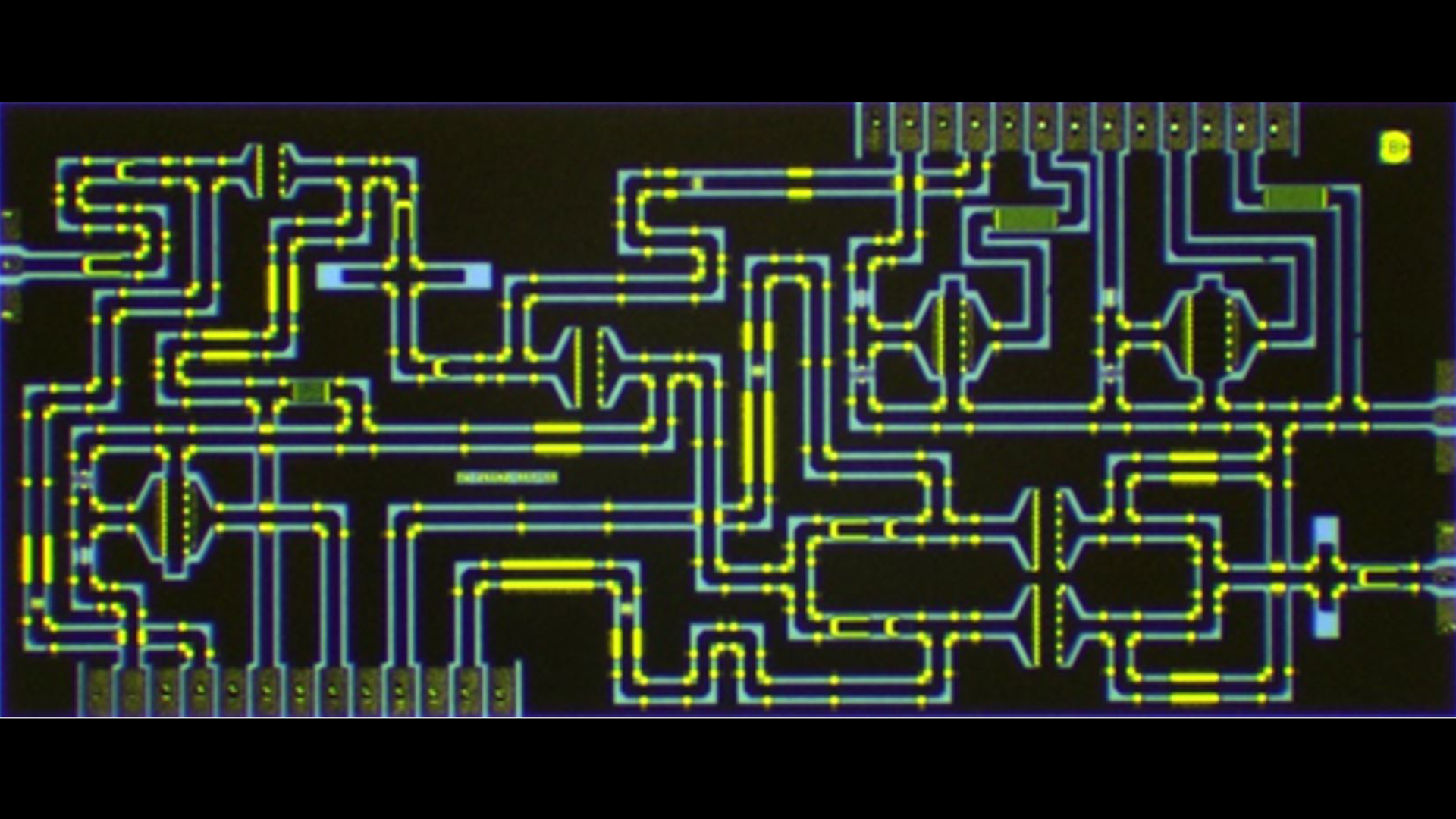
Fig. 1: Photograph of the fabricated MMIC.
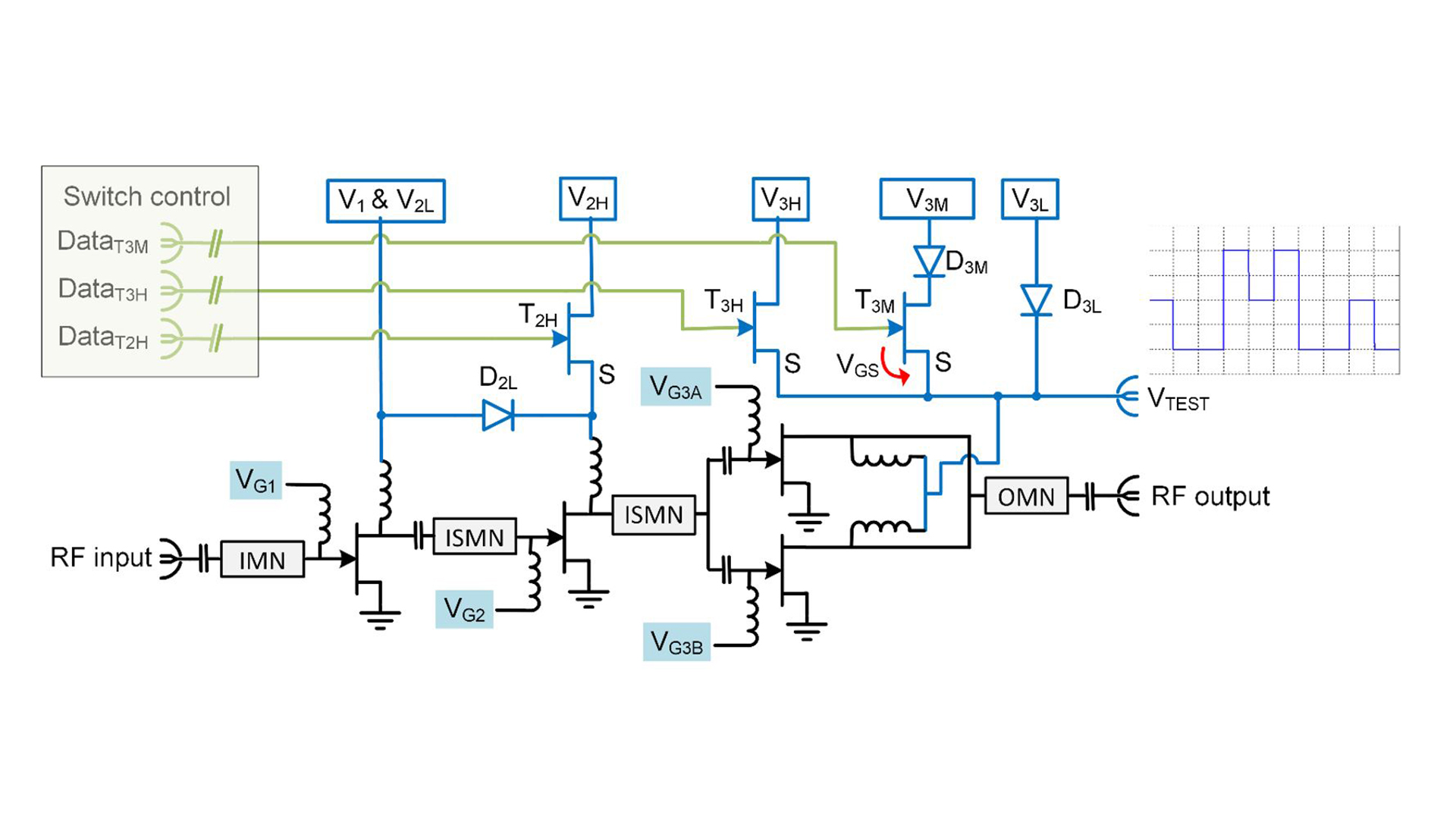
Fig.2: Simplified schematic of the three-stage integrated MMIC with a 2-level class-G integrated voltage switch for the 2nd stage and a 3-level class-G integrated voltage switch for the final stage.
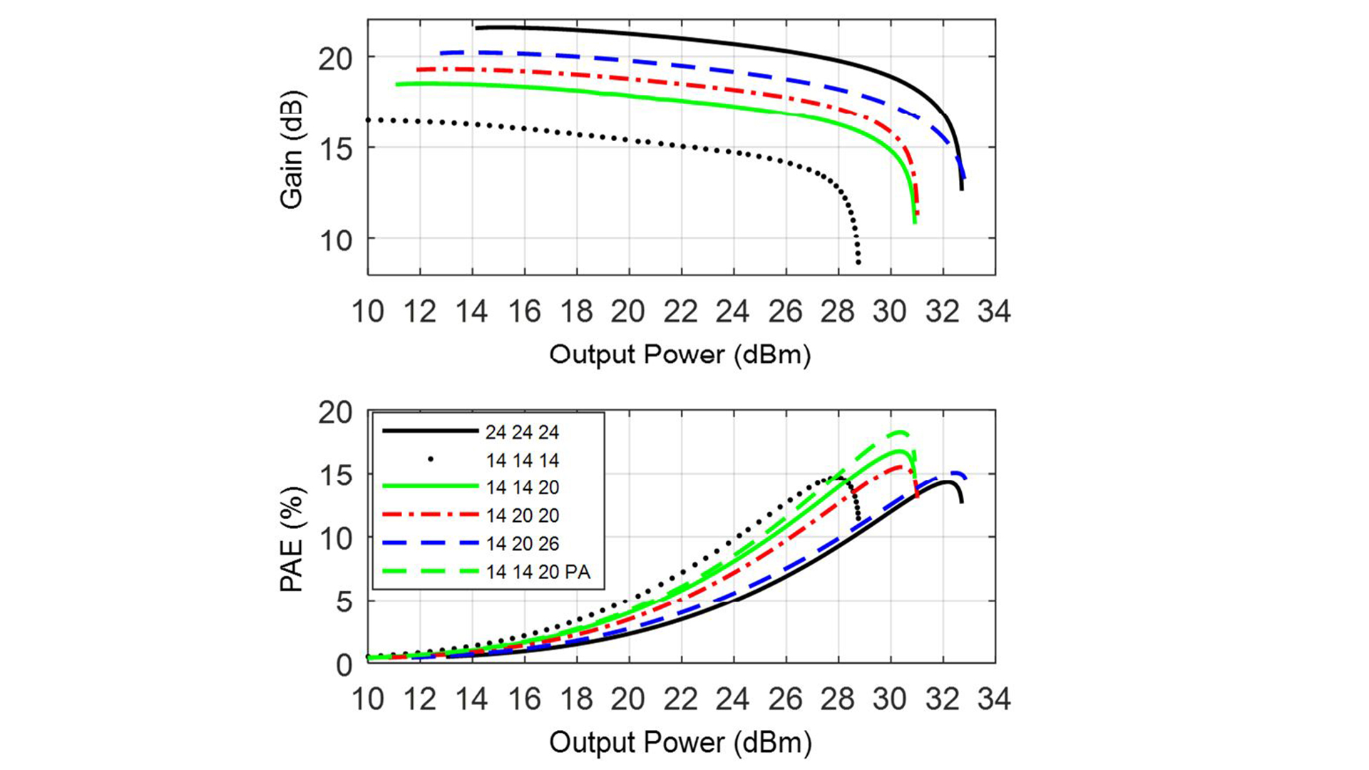
Fig.3: Gain and PAE versus output power at 26.4 GHz for combinations of 3 different supply voltages at IDQ1 and IDQ2 = 50 mA and IDQ3 at 100 mA.
In recent years, the focus of FBH’s RF Power Lab has been to transfer the knowledge and methods for efficiency enhancement implemented in discrete RF power GaN technology to integrated MMIC solutions for higher frequency applications.
A first approach with an integrated voltage supply switch on the PA chip was presented in [1]. Inspired by that concept, a 3-stage PA with a 2-level voltage supply for the second PA stage and a 3-level voltage supply for the final PA stage have been integrated on the same chip in novel design [2]. The topology with supply modulation of both the second stage and the final stage allows more flexibility in the performance optimization for alternative signals and frequencies.
The MMIC which is shown in Fig. 1 was fabricated using coplanar waveguide (CPW) technology in the 150 nm GaN-process at FBH with an integrated planar GaN-diode option. The 3-stage PA is scaled in the proportions 2:3:6 with an 8 x 50 mm transistor in the 1st stage, a 12 x 50 mm transistor in the 2nd stage and two combined 12 x 50 µm transistors with inter-transistor odd-mode stabilization in the 3rd stage. A simplified schematic of the MMIC topology is shown in Fig. 2.
The small-signal S-parameters show a 3-dB bandwidth from 24.4 to 28 GHz with input matching in the 5-10 dB range. The amplifier is unconditionally stable for the whole expected supply voltage range from 8 to 26 V. From sample measurements three fixed suitable supply voltages were selected, 14 V, 20 V, and 26 V. Hence, the 1st stage would run at 14 V the 2nd at either 14 V or 20 V and the 3rd at either 14 V, 20 V or 26 V. Each voltage supplied through its respective modulator path with its losses. The results can be seen in Fig. 3 with fixed 24-V supply for all stages as reference. As expected the linear gain varies a lot with supply voltage level and the output power is totally dominated by the 3rd stage supply. A maximum 5.5 %-points PAE improvement is found at about 5 dB back-off compared to the fixed voltage case.
The static influence of the switching stages was measured separately as the transfer characteristic of each PA stage. The diodes have considerable forward voltage drop of more than 1.5 V in the relevant current range. This is detrimental for the performance of the low- and middle-voltage stages. The effect on PAE was de-embedded for the peak PAE 14 V/14 V/20 V combination in Fig. 3. The dashed green line shows that the static losses of the switches cause 1.5 %-points PAE reduction.
The coming year will show the first dynamic results of discrete level supply modulation implemented for very high instantaneous modulation bandwidths in mm-Wave amplifiers. These achievements will outline the role for high efficiency GaN in future 5G telecom and space applications. The presented MMIC have highlighted the potential of mm-wave class-G solutions.
Publications
[1] O. Bengtsson, N. Wolff, S. Preis, F. Schnieder, S. Chevtchenko, W. Heinrich "GaN-HEMT MMIC with integrated Class-G Switching Stage for Discrete Level Supply Modulation for 20 GHz Space Applications", 2018 IEEE MTT-S Latin America Microwave Conference (LAMC 2018), 2018, pp. 1-3, doi: 10.1109/LAMC.2018.8699052.
[2] O. Bengtsson, S. Paul, C. Schulze, S. Chevtchenko, W. Heinrich "A 26 GHz GaN-MMIC with Integrated Switches for Discrete Level Supply Modulation", 2021 IEEE/MTT-S International Microwave Symposium (IMS), 2021, pp. 527-530.