Si doping to reduce strain and improve crystal quality of AlN layers – a route to enhanced UV LED efficiency
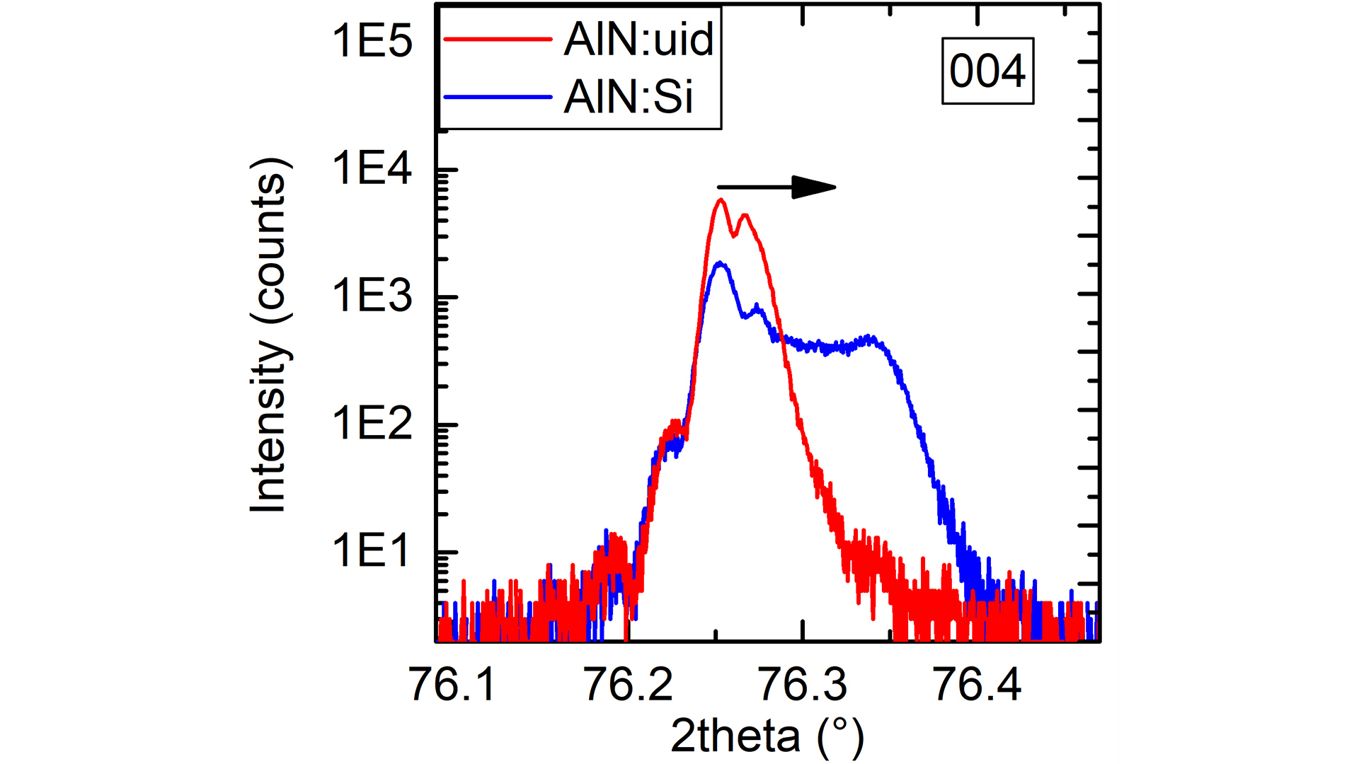
Fig. 1: HRXRD 2theta/theta measurements of the 004 reflections of 1.8 µm MOVPE-AlN grown on HTA-AlN. The arrow indicates relaxation towards less compressive values.
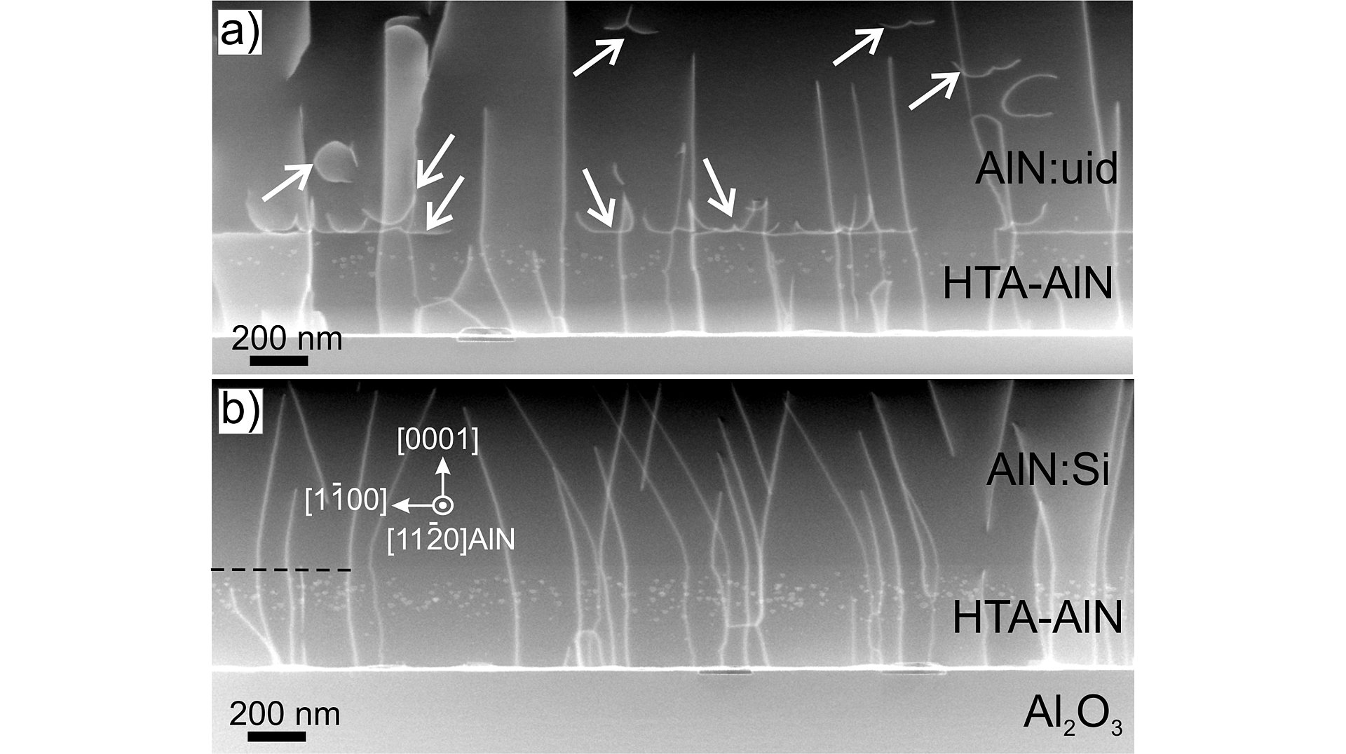
Fig. 2: Cross-sectional ADF STEM images of (a) AlN:uid and (b) AlN:Si. White arrows in (a) point to dislocation half-loops, propagating from the surface in the undoped AlN:uid layer. These defects are absent in the AlN:Si layer shown in b).

Fig. 3: a) ADF STEM images of AlN:uid/HTA-AlN interface. b) Sketch with a classical model of dislocation half-loop nucleation at the layer surface; c) Sketch explaining the experimentally observed irregular half-loop shape.
AlGaN-based light emitting diodes (LEDs) operating in the ultra-violet (UV) wavelength range can be used for skin-tolerant inactivation of multi-resistant bacteria and viruses, including SARS-CoV-2. To enhance the efficiency of such UV LEDs, AlN templates with a low threading dislocation density (TDD) are required. Generally, the growth of AlN layers takes place on sapphire substrates with a different crystal structure, whose lattice constants differ from those of AlN. This results in AlN layers exhibiting a high TDD in the range of 1010 cm-2, which strongly affects the device efficiency. One of the most efficient ways to reduce the TDD of the defect-rich AlN template layers is to anneal them at high temperatures in an N2 ambient, the so-called high-temperature annealing (HTA) technique. The AlN layers treated with HTA (HTA-AlN) show not only strongly reduced TDDs, but also a decrease of the in-plane lattice constant. A further overgrowth of such low-TDD templates by AlN and by AlGaN is necessary to achieve the required UV LED heterostructures.
In our recent experiment we have shown that a further overgrowth step with AlN using MOVPE leads to enhanced compressive strain, an increased wafer curvature, and subsequent relaxation by formation of new defects, the so-called dislocation half-loops. With increasing AlN thickness, these defects are continuously formed at the layer surface and propagate through the layer down to the homoepitaxial MOVPE-AlN/HTA-AlN interface. This drastically decreases the layer quality and makes the use of these layers in LEDs inappropriate. To solve the problem of enhanced defect formation, we have introduced Si doping during homoepitaxial MOVPE overgrowth of the HTA-AlN templates. This led to a strong inclination of threading dislocation lines pre-existing in the HTA-AlN layer. Such dislocation movement reduces the compressive strain during growth. It also allows to achieve a higher strain relaxation and to completely avoid the formation of unfavorable and hardly controllable dislocation half-loops. Our experiment demonstrates a way towards a modified strain state and a better crystalline quality of the AlN layers and can be used to further improve subsequent AlGaN epitaxy.
This work was partially supported by the German Federal Ministry of Education and Research (BMBF) through the consortium “Advanced UV for Life” under project contract 03ZZ0134B.
Publication
Mogilatenko, S. Walde, S. Hagedorn, C. Netzel, C.-Y. Huang, M. Weyers, “Impact of Si doping on dislocation behavior in MOVPE-grown AlN on high-temperature annealed AlN buffer layers”, J. Appl. Phys., vol. 131, no. 4, pp. 045702, doi:10.1063/5.0073076 (2022).