Paving the way for next-generation power converters – processes towards vertical GaN and β-Ga2O3 FinFETs
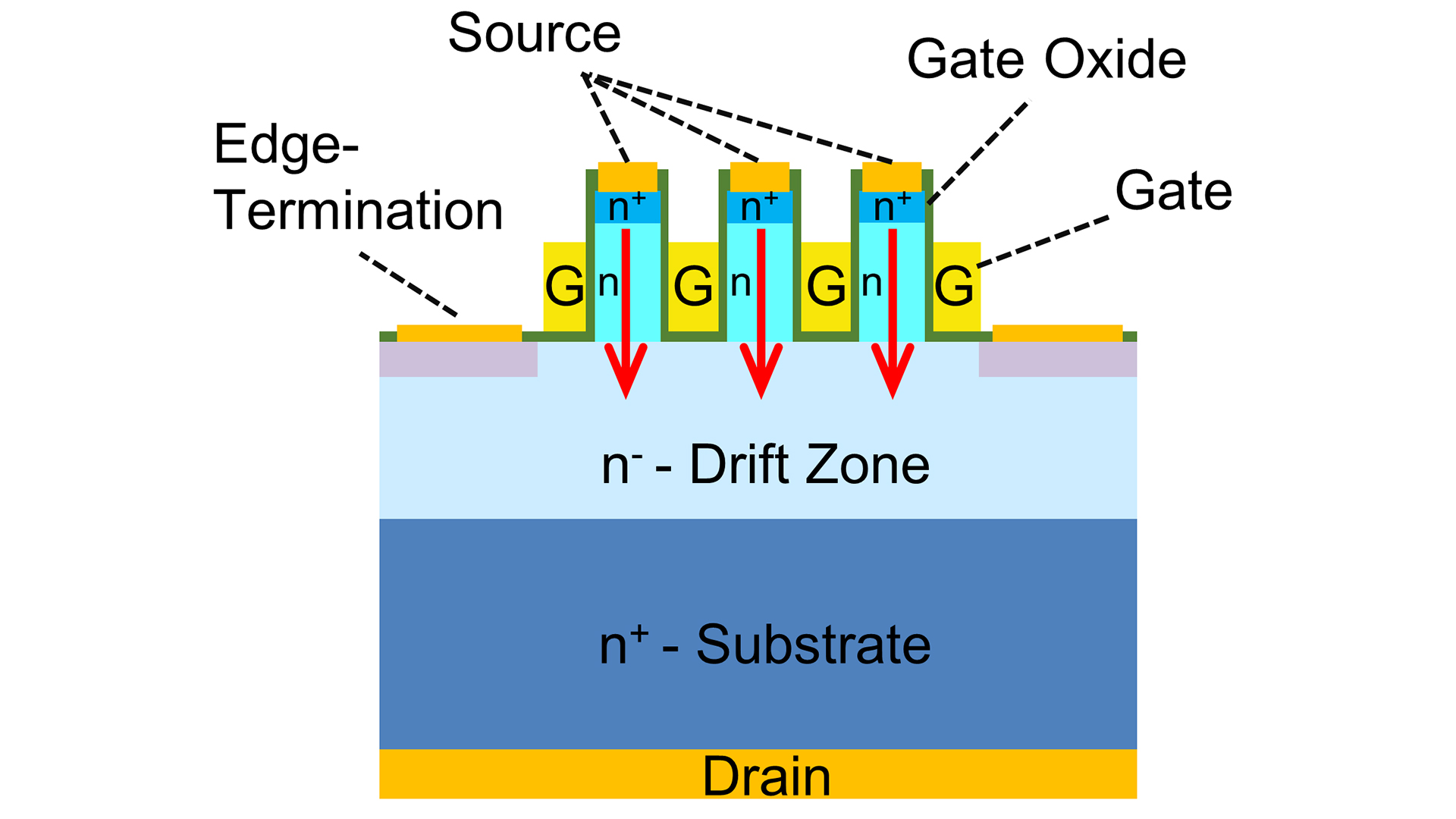
Fig. 1: Schematic cross section of a vertical FinFET device.
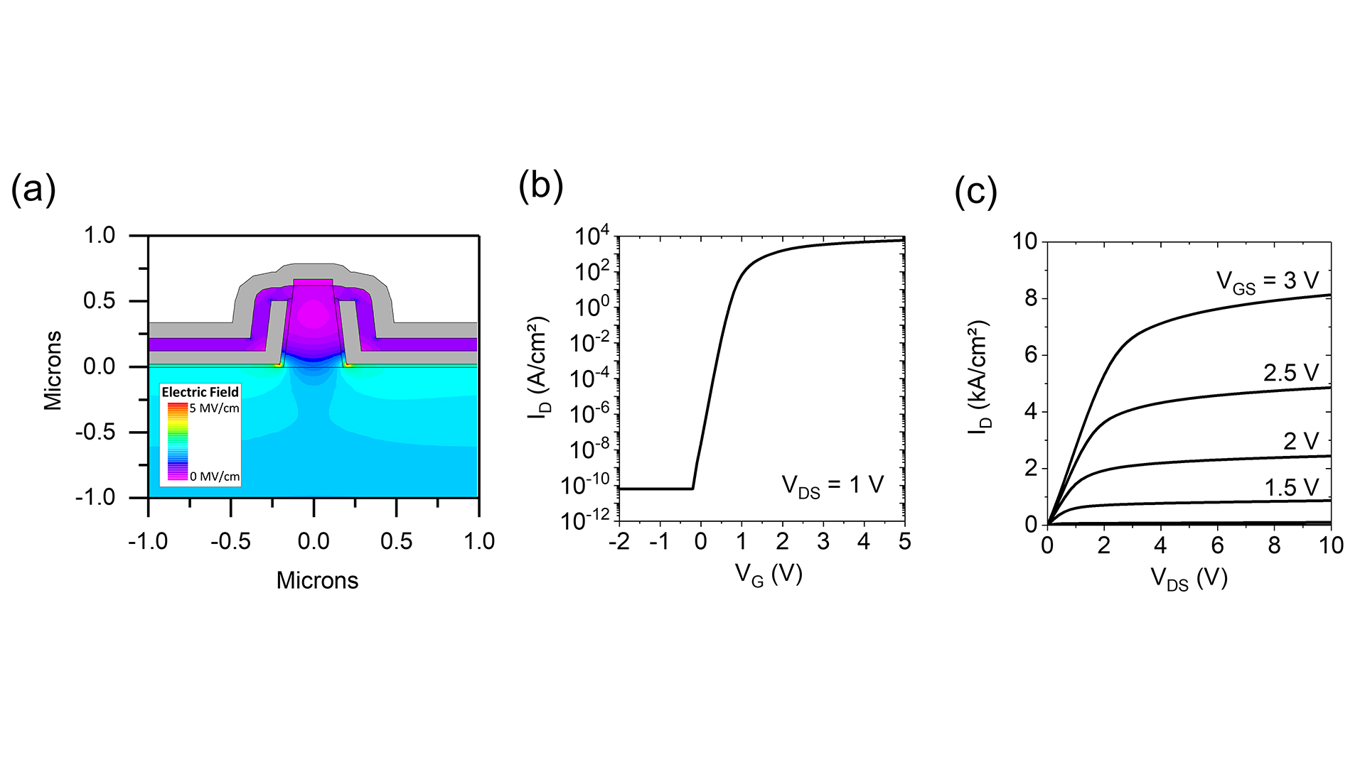
Fig. 2: (a) Electric field distribution of a β-Ga2O3 FinFET with a doping concentration of the 3 µm thick drift zone layer and in the fin region of 2 × 1016 cm-3 at a blocking voltage of 400 V. Simulated (b) transfer and (c) output curves for the vertical β-Ga2O3 FinFET.
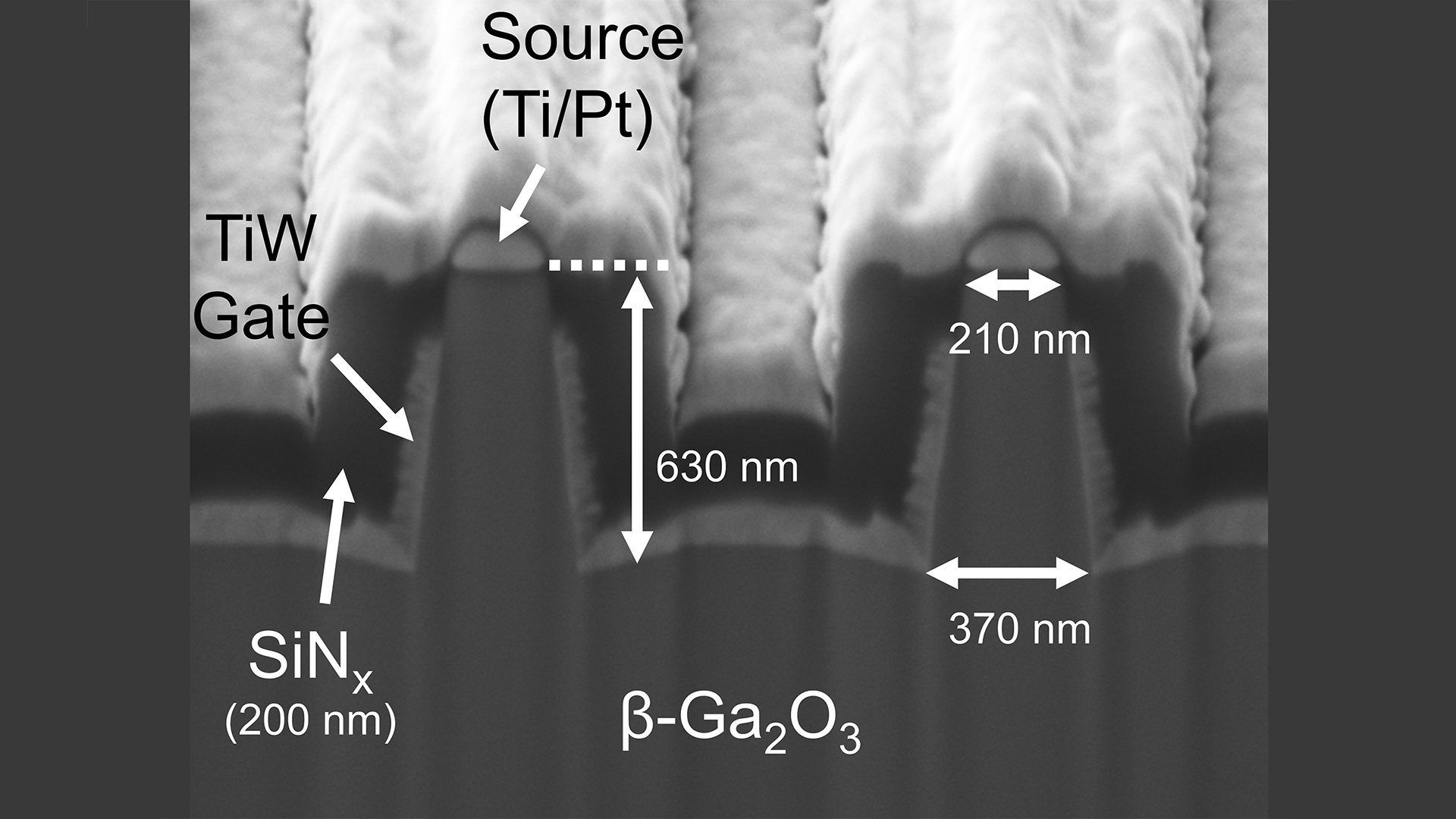
Fig. 3: Scanning electron microscopy (SEM) cross-section image of FinFET structures realized in β-Ga2O3.
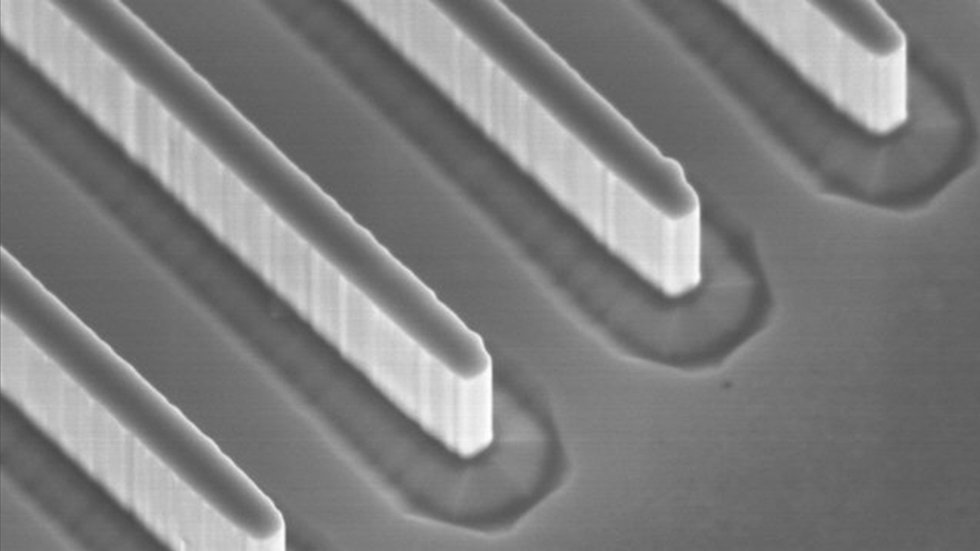
Fig. 4: SEM micrograph of structured fin channels realized on GaN.
The research and development of energy-efficient semiconductor power converters for converting electricity in everyday electronic applications is an important aspect in order to save energy and thus reduce CO2 emission. More than 50 % of the world-wide generated electricity has to be converted by semiconductor power converters. Thus, an increase in efficiency by only a few percent can save enormous amounts of primary energy. In this regard, wide bandgap semiconductor devices – transistors and diodes – as explored at FBH are playing a key role in these kinds of developments. They have the potential to reduce the power converter volume by 50 % and raise efficiency levels up to 99 %. This corresponds to reducing the size of a laptop power supply to the scale of a mobile phone charger. Semiconductors such as gallium nitride (GaN) or beta-gallium oxide (β-Ga2O3) feature a very high breakdown strength. Hence, they enable power switching devices with unprecedented power densities and low switching losses – the most important conditions for being efficient.
Up to now, lateral device concepts have been successfully used to realize power converters using GaN or β-Ga2O3. However, this concept has certain drawbacks; especially when aiming for very high breakdown voltages >1 kV as the device dimensions directly scale with increasing breakdown voltages. A much better approach which overcomes this issue is the use of a vertical device structure such as a vertical fin field-effect transistor (FinFET), as shown in Fig. 1. Here, the breakdown voltage only depends on the drift layer properties, such as thickness and doping concentration. These parameters are defined during the epitaxy process, making the breakdown voltage almost independent from the actual device area. This concept also enables an ideal separation of the high potentials on top and bottom of the epitaxial wafer, allowing to target blocking voltages beyond 1 kV. In addition, several other positive aspects become obvious such as superior reliability or improved thermal management compared to a lateral device structure.
In this regard, FBH has recently started research activities to develop vertical power transistors based on the wide bandgap semiconductors GaN and β-Ga2O3. The transistor fabrication is supported by numerical device simulation using Silvaco Atlas, as shown in Fig. 2, thus iteratively optimizing the fabrication process. The simulator allows to calculate various device-related parameters such as the field distribution inside the device, revealing certain weakness points. The current density level of such devices is expected to exceed several kA per cm² as derived from simulation results.
Furthermore, a first process sequence for the fabrication of such vertical FinFETs based on β-Ga2O3 has been experimentally established, which is shown in the representative cross-section in Fig. 3. The key technology steps include using high-resolution e-beam lithography to define the sub-micron fin structures as well as deep dry etch processes to achieve steep sidewalls with a high aspect ratio. Fig. 4 depicts a scanning electron micrograph of 200 nm wide structured fins realized in GaN. In addition, a sophisticated photoresist planarization process has been developed in order to realize the structured sidewall gate topology.
In conclusion, this novel technology approach will open the possibility to use the full potential of the material properties of the wide bandgap semiconductors GaN and β-Ga2O3. It is expected that such developments will pave the way for next-generation power converters with high efficiencies at voltage levels far beyond 1 kV.
This work was funded by the Federal Ministry of Education and Research in Germany (BMBF) within the framework of the joint research project OXIKON, Funding No. 03VP03711 and the Research Project GoNext, Funding No. 16ES1084K as well as by the KDT JU Grant No 101007229: The JU receives support from the European Union’s Horizon 2020 research and innovation programme and Germany, France, Belgium, Austria, Sweden, Spain, Italy.