Low power in mind: electrical and structural improvements of the Pd/p-GaN interface
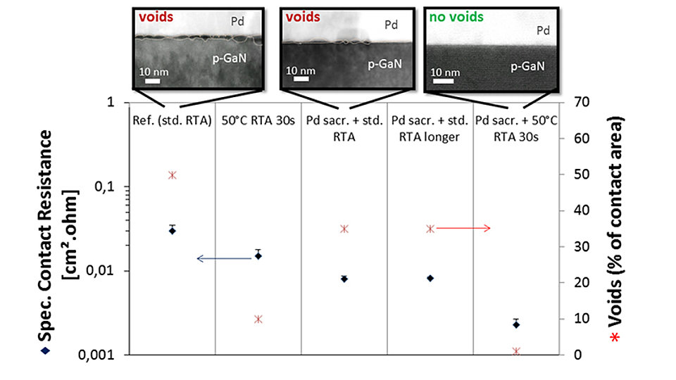
Fig. 1: Specific contact resistance and % of voiding at the Pd/p-GaN interface for selected annealing processes. From the exemplary STEM images, the area of voids is extracted. The annealing process (D) 50°C steps held for 30 s combined with the sacrificial Pd layer is the best combination for this system.
Optoelectronic devices should offer not only a long lifetime and great reliability, but ideally also low power consumption. Low operation voltage, which reduces the power consumption, requires low contact resistance between the contact and the semiconductor material. The p-contact metal and its subsequent treatments are – in addition to effective high p-doping and good crystal quality – of great significance to lower the resistance. At FBH, we have taken a closer look [1] at the respective contact system at the Pd/gallium nitride (GaN) interface to achieve low ohmic p-contacts.
Pd is – next to Ni/Au – often chosen for contact formation on the wide band gap material. However, reliable and reproducible Pd/p-GaN ohmic contacts are inherently challenging because of the presence of micro-voids observed at this interface. We were able to improve the quality of the contact system by a systematic analyzation and optimization of the surface cleanliness as well as the annealing parameters, leading to void-free and clean interfaces with ohmic behavior.
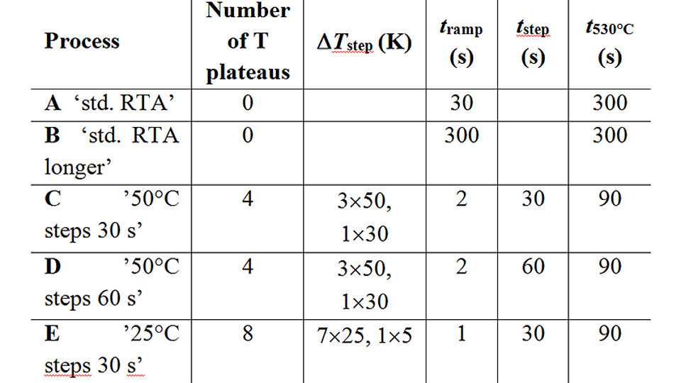
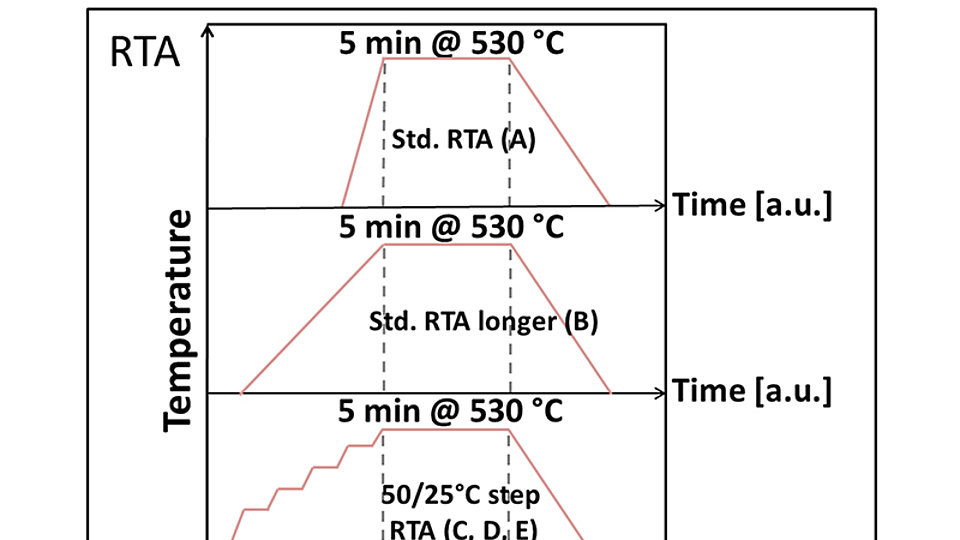
Scanning transmission electron microscopy (STEM) data show that micro-voids at the Pd/p-GaN interface form during rapid thermal annealing. A combination of the following effects is suggested to support the void formation: (1) the differences in thermal expansion coefficients of the materials, (2) excess matrix or impurity atoms in the semiconductor, at the interface, and in the metals, which are released as gases and (3) the strong anti-surfactant effect of Pd on Ga-rich p-GaN surfaces. We found that a slow temperature ramp during contact annealing reduces the formation of voids likely by suppressing the accumulation of gases at the interface. Table 1 summarizes the annealing variations.
STEM images and TLM analysis (Fig. 1) from all samples show that the area of the voids at the metal/p-GaN interface is reduced by applying a step-wise heating of the sample (process D). This significantly reduces the specific contact resistance (by TLM) of the Pd/p-GaN contact.
However, another important influence on the contact resistance is the surface cleanliness of the GaN prior to metal deposition. By applying a Pd sacrificial layer, which is then etched in aqua regia before the final p-contact is deposited, the voiding can be eliminated completely. XPS data show that the Ga/N ratio can be reduced to approximately 1 by this sacrificial layer process. Thus, excess Ga is removed from the interface. The specific contact resistance is reduced by an order of magnitude to 2x10⁻³ Ωcm² at 1 mA for the same epitaxial layer stack.
Therefore, we suggest that a strong anti-surfactant effect of a Ga-rich p-GaN surface, together with thermal out-diffusion of gaseous species (most likely H) from the layer stack, lead to accumulation of gases, hence void formation, at the Pd/p-GaN interface.
As a result, the quality of the contact system is improved by the systematic optimization of the surface cleanliness as well as the annealing parameters, reflecting in a voids-free interface with reduced contact resistances and a reduction of the driving voltage (at 2 A) by 2 V.
This work was supported by the European Fund for Regional Development of the European Union in the framework of the Berlin-Polish joint projects “Brilliant high power violet emitting laser diodes (BriVi)” and “From UV to blue – Reliable laser sources for environmental monitoring (RelyLa)” administrated by the Investitionsbank Berlin within the “Program to promote research, innovation and technologies” (ProFIT) under contracts 10157699 and 10164535, respectively. Further support was given by the German Federal Ministry of Education and Research (BMBF) in the framework of the KMU-innovative project “AlGaInN laser diodes and tapered amplifiers in the near UV (UVMOPA)” under contract 13N13023.
Publication
[1] M. Norman-Reiner, E. Freier, A. Mogilatenko, I. Ostermay, V. Hoffmann, R. Szukiewicz, O. Krüger, D. Hommel, S. Einfeldt, M. Weyers, G. Tränkle, "Structural and Electrical Properties of Pd/p-GaN Contacts for GaN-based Laser Diodes," J. Vac. Sci. Technol. B 38 (3), 032211 (2020).


