In-line control of waveguide structures for non-linear optical processes
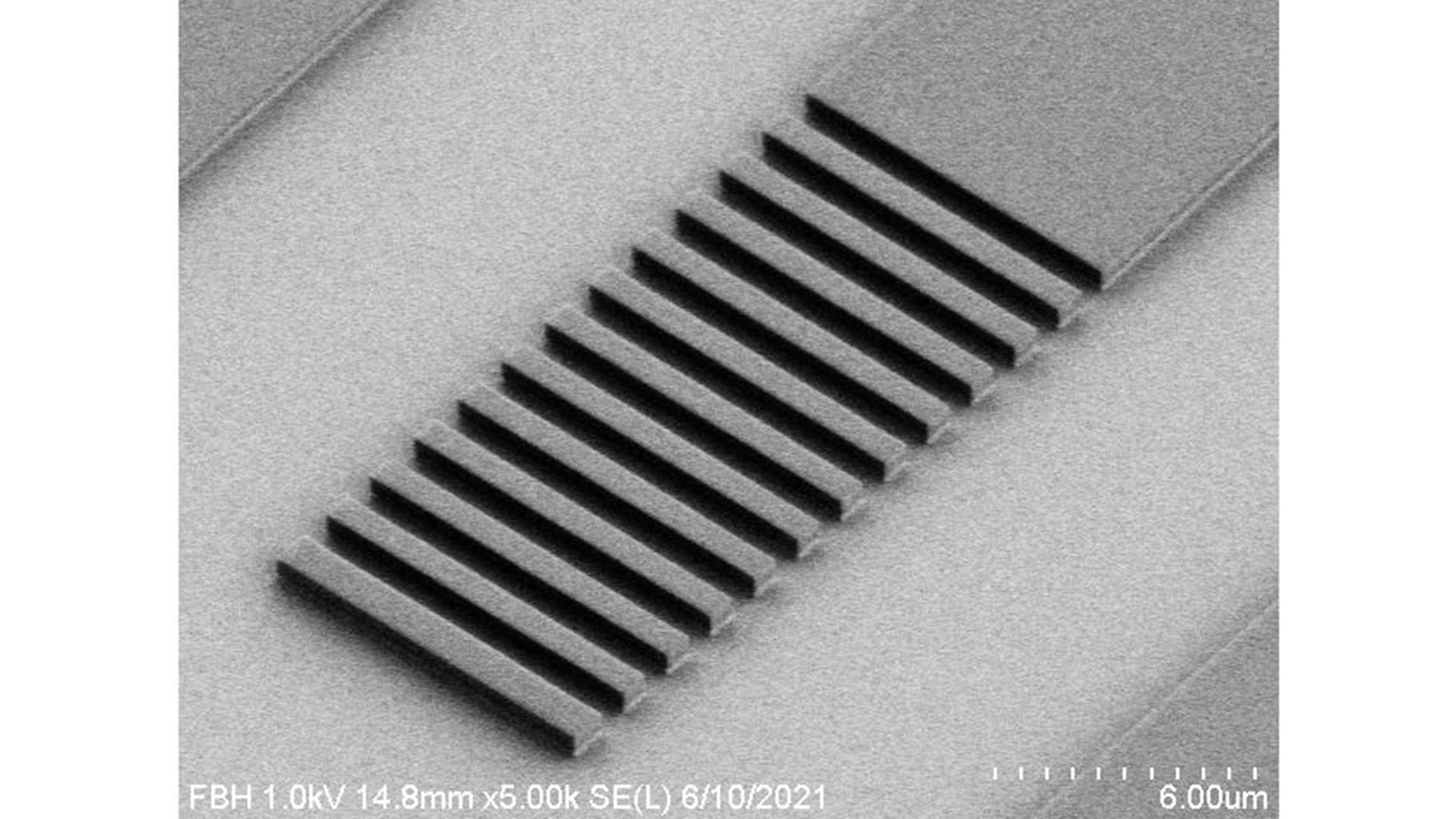
SEM image of an AlGaAs waveguide with an optical grating coupler
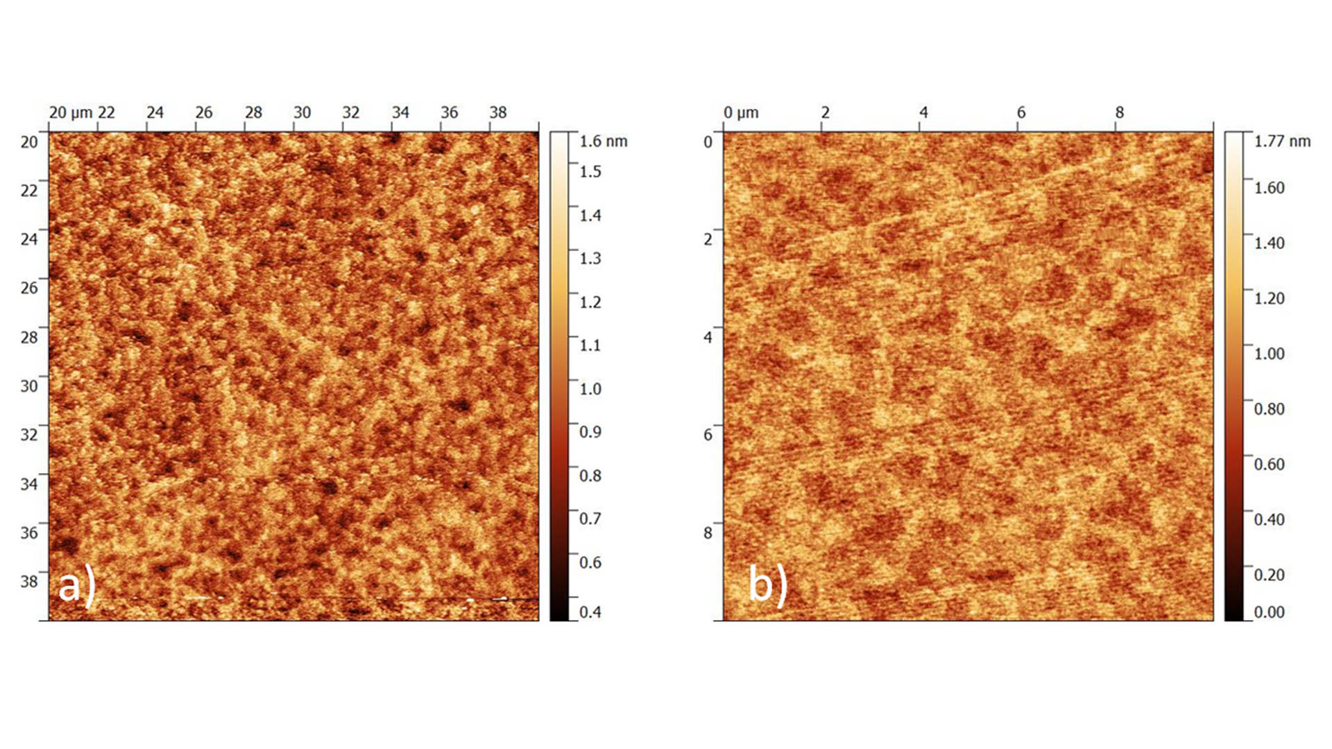
Fig. 1: High resolution surface roughness characterization by contact mode AFM imaging of an AlGaAs layer (a) after epitaxial growth of the layer and (b) after etching the surface to prepare the desired waveguide structures, showing a typical roughness of 0.3 nm rms.
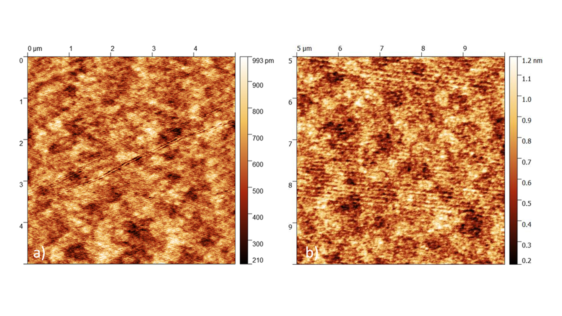
Fig. 2: Surface roughness characterization of an InGaP layer acquired similar to Fig. 1; (a) after epitaxial growth of the layer and (b) after etching, showing a typical roughness of 0.2 nm rms, indicating the improved surface quality.
Non-linear optical processes such as second harmonic generation and spontaneous down conversion take place in waveguides with tiny cross sections and high index contrast. The semiconductor AlGaAs is well known for its suitable properties to form waveguide structures, which can be used as single photon sources for quantum optical experiments. Therefore, we use AlGaAs to create optical structures for non-linear processes.
To achieve a high efficiency of these devices, a minimization of optical losses within the waveguides is required. Typically, the injected light is lost by scattering at slightly rough edges of the waveguides, which makes surface roughness values below 0.3 nm rms necessary. The AlGaAs waveguide material is grown epitaxially by means of MOVPE. Subsequently, the desired cross section of the waveguide is defined in a wet chemical process. Optimization and monitoring of this process focusses on preserving the low surface roughness provided from the epitactic growth process.
To identify critical process steps and to monitor improvements in our preparation process, we rely on the characterization of the surface roughness by atomic force microscopy (AFM). To this end, we now have a new AFM with low noise and low drift available at FBH, which allows for a high resolution in-line control of optoelectronic devices and other samples within minutes. It offers simple and consistent results by the availability of a wide range of preconfigured settings. On the motorized sample stage of the system, specimens of a diameter of up to six inches can be mounted and addressed.
This new technology now has been used to monitor the interface quality during the different steps of the preparation process for our optical waveguides. By characterization of surfaces at different individual process steps in contact mode AFM, we were able to confirm that stopping the wet etching on intermediate epitaxy layers of InGaP preserves their smoothness while when stopping on AlGaAs, a significant increase of roughness has been observed. As a consequence, transmission losses in our systems could be significantly reduced by wrapping the AlGaAs waveguides in thin InGaP boundary layers.