Extended processing capabilities: through silicon substrate etching at cryogenic and room temperatures
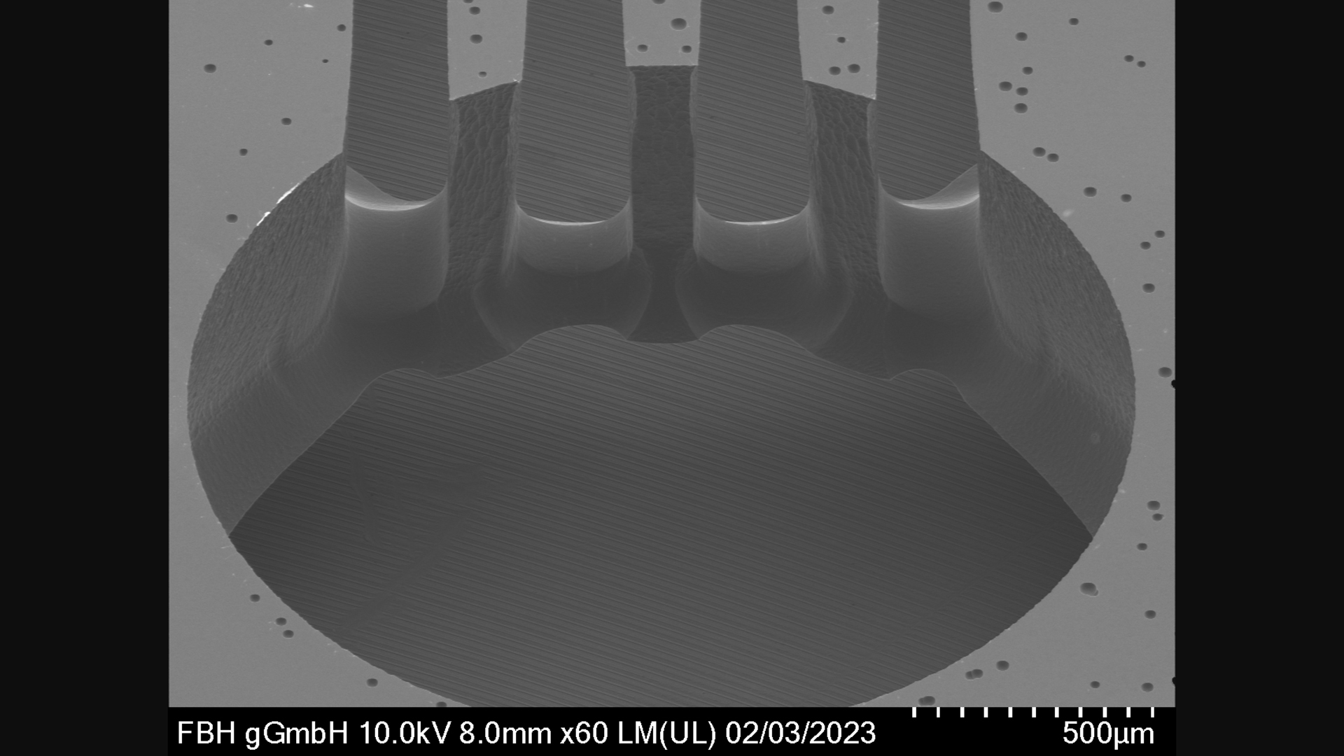
Fig. 1: Tilted image of a round shaped opening through a 1 mm Si wafer. The wafer carrier is visible through the hole. At the top of the image one hole is connected to another through four trenches.
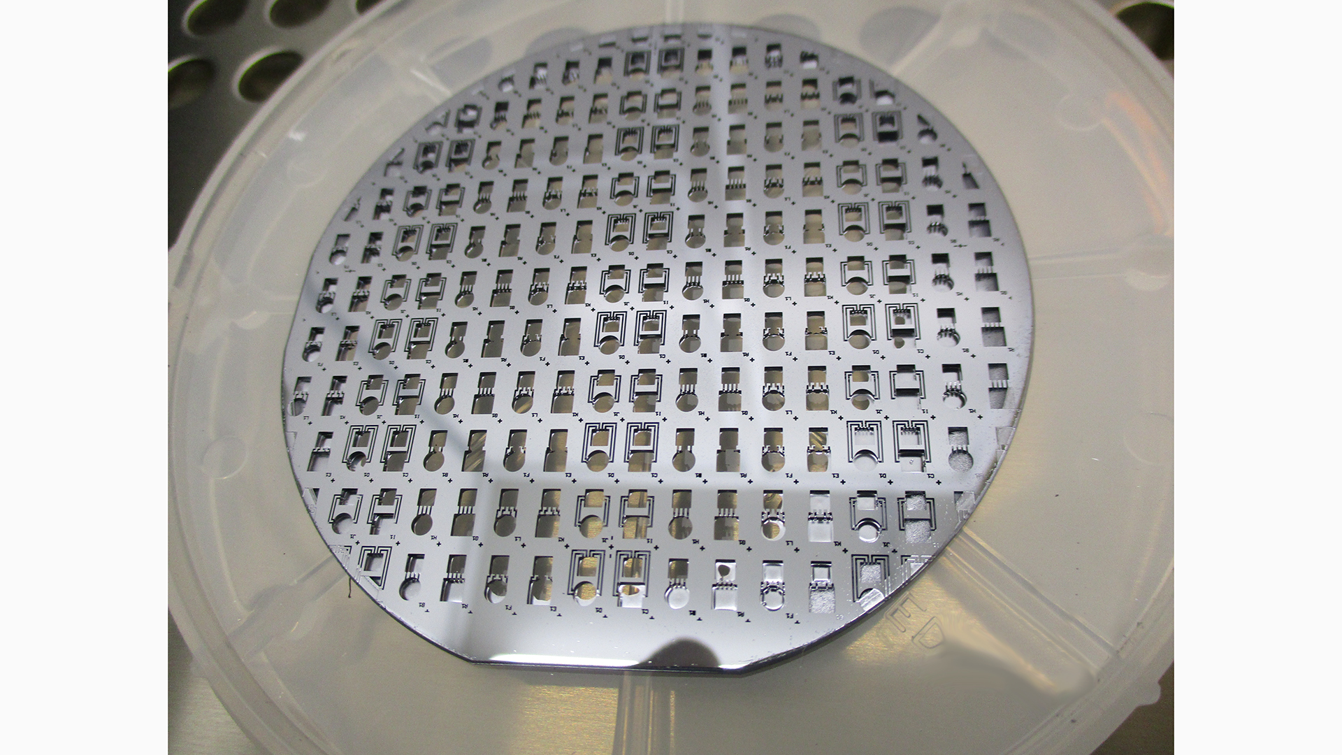
Fig. 2: Image of a completely opened 1 mm thick silicon wafer. Only 80 nm of ALD-Al2O3 hard mask is necessary to etch through the silicon. The ALD-Al2O3 hard mask was removed by wet chemical etching. To fabricate micro gas cells, the wafer will be bonded to glass substrates.
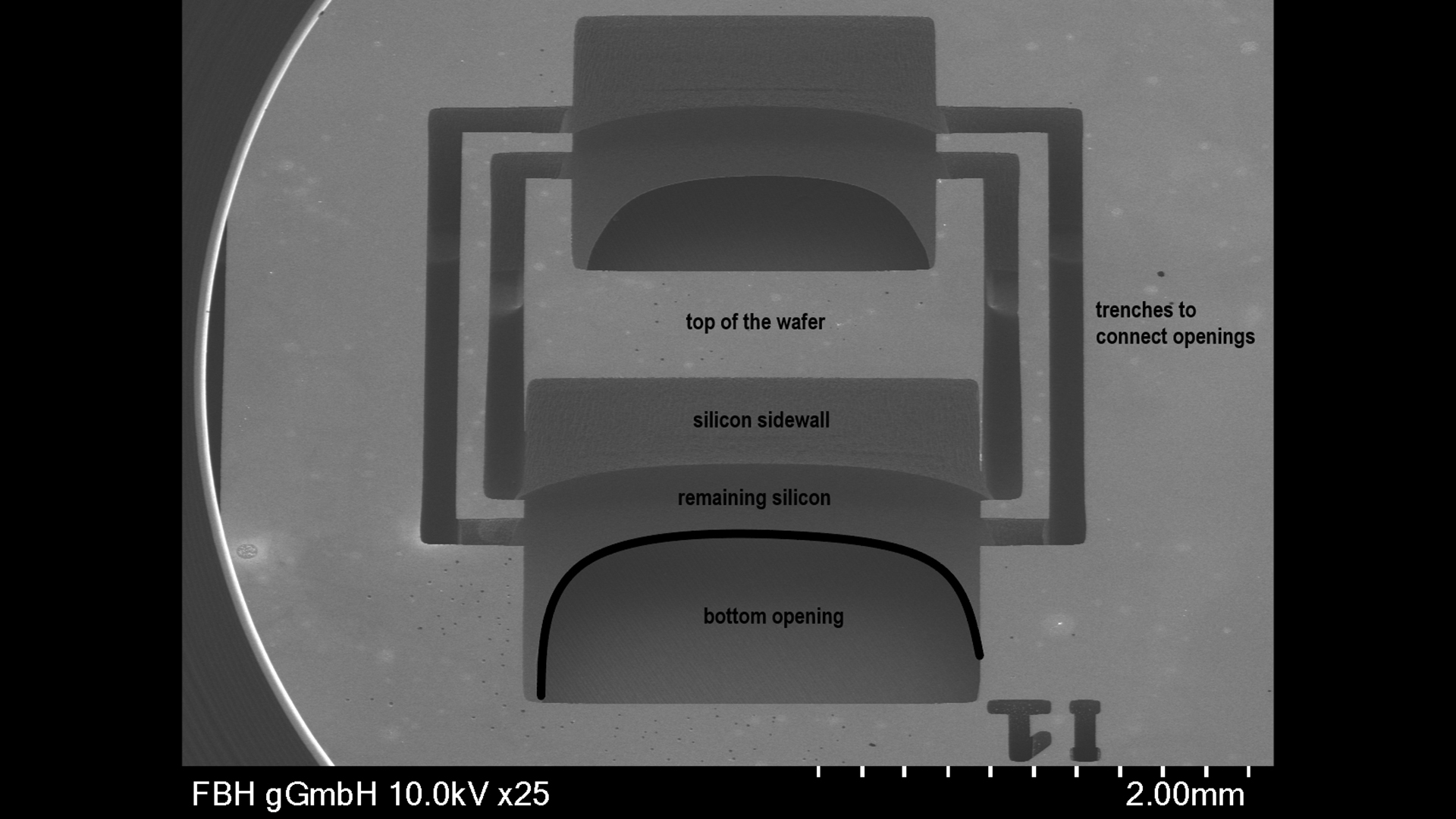
Fig. 3: Tilted SEM image showing details of an opened shot in a 1 mm thick silicon wafer processed with a single run Bosch process. Hard mask and backside metallization are removed. On top and bottom one can see two rectangular openings through the wafer. Both openings are connected via four trenches that were etched together in the same run.
Research at FBH is focused on electronic and optical components, modules, and systems based on compound semiconductors. To expand our capabilities for processing semiconductor materials, we have procured a dedicated plasma etch processor for silicon wafer processing. This deep reactive ion etching (DRIE) tool opens up new capabilities for the institute, which are particularly important, e.g., to form through-silicon vias used to integrate InP-based devices with silicon [1] and to fabricate micro gas cells [2]. Sentech Instrument’s dry etcher SI 500 DRIE is able to process wafers up to 200 mm diameter. The tool allows to operate in two different process modes using various process gases like Ar, SF6, O2, C4F8, N2, and CHF3. For the cryogenic mode, the etcher is equipped with a special cooling system, which uses liquid nitrogen to cool the electrode down to -100 °C. The second option is the so-called Bosch process using alternating gas flows of SF6 and C4F8, thereby enabling deep anisotropic etching into silicon at room temperature.
The challenge when producing micro gas cells was to fabricate windows of approximately 2 x 2 mm² in 1 mm thick silicon wafers, i.e. to etch completely through the wafer. We used typical 4-inch 525 µm thick silicon wafers at the beginning of the process development. For this task, we chose the Bosch process, which required to balance between etching steps and sidewall passivating steps that would either lead to non-wanted isotropic etching or to an etch stop because of over passivation, respectively. The process window found for 525 µm thick wafers also worked well for 1 mm thick silicon (Figs. 1 and 2). We obtained vertical and very flat side walls.
For the deep etching, we had to find the right masking material. First tests with a thick photoresist mask led to cracking of the resist. We improved this process by replacing it with a more resistant silicon oxide (SiOx) mask. This way, we achieved an etch selectivity of 250:1 (Si:SiOx), which was not sufficient because a hard mask thickness of at least 4 µm is necessary to etch 1 mm Si. However, we could not deposit this in an efficient way. Looking for an alternative masking material, we found a solution in using an atomic layer deposited Al2O3 hard mask. Using a substrate temperature of 5 °C, we could achieve a significantly higher selectivity of >13,000:1 (Si:ALD-Al2O3) than for Si:SiOx. The much higher etch selectivity is due to fluorination of the Al2O3 mask during the process, which forms a stable top layer at lower temperatures. Hence, only 80 nm of Al2O3 was sufficient to etch through the entire 1 mm silicon wafer. To keep the substrate at the given temperature, we realized backside cooling by a helium backside flow. However, this well-established cooling technology proved to be an obstacle. When etching completely through, i.e., when opening the first holes in the wafer, the helium could pass through the opened holes thereby diluting the plasma and stopping the etch process. To overcome this impediment, a 200 nm thick aluminum backside metallization was applied that works both as etch stop for the silicon etch process and also as efficient barrier for the helium flow. We were able to easily remove both etch mask and backside metallization by wet chemical etching.
The results obtained here pave the way for the fabrication of vapor cells for optical frequency reference devices and will be the basis for novel concepts of semiconductor devices and systems.
Publications
[1] D. Stoppel, I. Ostermay, M. Hrobak, T. Shivan, M. Hossain, M. Reiner, N. Thiele, K. Nosaeva, M. Brahem, V. Krozer, S. Boppel, N. Halder, N. Weimann, “NiCr resistors for terahertz applications in an InP DHBT process”, Microelectronic Engineering, Vol. 208, 1-6 (2019), https://doi.org/10.1016/j.mee.2019.01.007.
[2] A. Strangfeld, B. Wiegand, J. Kluge, M. Schoch, M. Krutzik, "Compact plug and play optical frequency reference device based on Doppler-free spectroscopy of rubidium vapor," Opt. Express 30, 12039-12047 (2022), https://doi.org/10.1364/OE.453942.