Diamond nanopillars with incorporated single photon emitters for quantum technologies
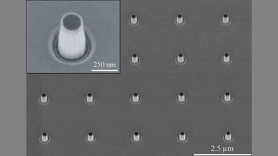
Fig. 1: Scanning electron micrograph showing a tilted view of the fabricated nanopillars, each with a diameter of about 200 nm and about 500 nm height. Inset: close-up view of a single nanopillar.
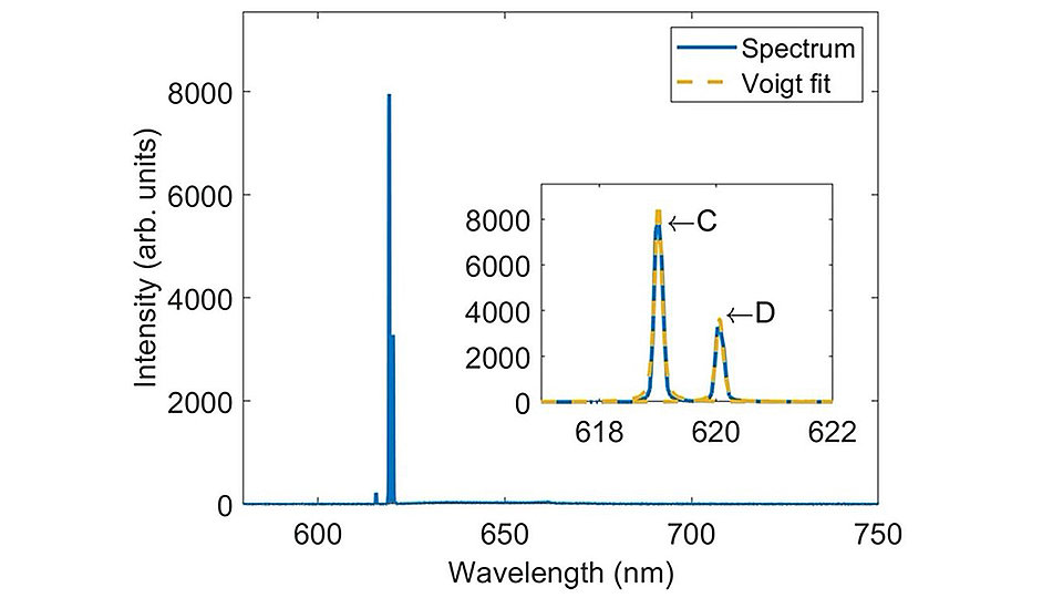
Fig. 2: Data plot of the spectrum of a single SnV defect centerre at a temperature of about 8 K. Inset: zoom into the spectral range of the zero phonon line of an SnV, peaks C and D originate in fluorescence from these zero phonon lines.
For the application of optical quantum technologies, high-efficiency single photon emitters are required. One of the most promising single photon sources are defect centers in diamond which can be operated both at room as well as cryogenic temperatures. Through the incorporation into diamond nanostructures, the highest optical efficiencies can be achieved.
The Ferdinand-Braun-Institut has now succeeded in fabricating nanostructures in diamond that have the shape of pillars and are therefore called nanopillars. A 2 x 2 µm2 grid of such nanopillars, each with a diameter of about 200 nm, is visualized in a scanning electron micrograph in Fig. 1. For the diamond patterning, oxygen plasma was used in an inductively coupled plasma etcher.
The nanopillars act as waveguides for light that is generated by laser irradiation via a single photon emitter located right at the center of the nanopillar. The nanopillars enable the efficient collection in an optical microscope, which is crucial for a variety of applications in quantum technology.
A single photon emitter is a very faint light source that only emits the smallest unit of light: one photon at one point of time. In contrast to classical light sources, e.g., LEDs or lasers, single photons obey different photon statistics and are therefore suited for secure communication and optical quantum simulations.
Before the nanopillars were etched into the diamond substrate, which typically has dimensions of 3 x 3 x 0.3 mm3, single tin-vacancy (SnV) defect centers were fabricated through ion implantation of tin and subsequent annealing at 1050ºC. The implantation was carried out at FBH, annealing was done in Prof. Kai Müller’s group at the Walter-Schottky Institute, Technical University Munich. In contrast to typical implantation doses of 10^12 to 10^16 ions/cm2 used in semiconductor fabrication, the dose of tin implantation was only about 10^11 ions/cm2. During the annealing process, single lattice vacancies in diamond are mobilized and diffuse through the diamond lattice. Due to a lower bonding energy, these lattice vacancies can combine with the implanted tin ions to form a SnV defect center at random lateral positions. After the nanopillar fabrication laser scanning methods and spectroscopic analysis are applied to determine if SnV defect centers were incorporated into the pillar. A typical spectrum of a single SnV defect centeris shown in Fig. 2.
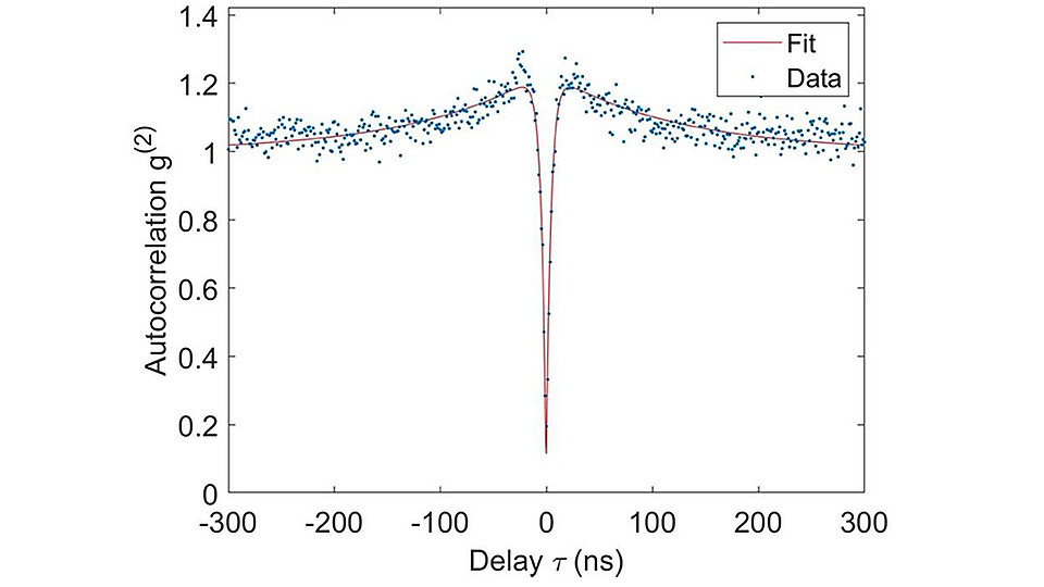
The experimental verification that the light emitted from an SnV defect center inside a nanopillar is indeed of quantum nature is performed with so-called autocorrelation measurements. In case that single photons are collected, the second-order autocorrelation function g(2)(t) exhibits a dip at t=0. A typical g(2)-function is plotted in Fig. 3, values of g(2)<1 indicate the quantum nature of light as is confirmed here.
The use of the SnV-nanopillar structures made at FBH for quantum technology application is presently under further development.
The discussed results were realized within the project “Diamant-Nanophotonik für On-Chip Quantentechnologien” (DiNOQuant, project number 13N14921) supported by the Federal Ministry of Education and Research of Germany (BMBF).


