Deep UV LED wafers with reduced bow by applying focused laser patterning
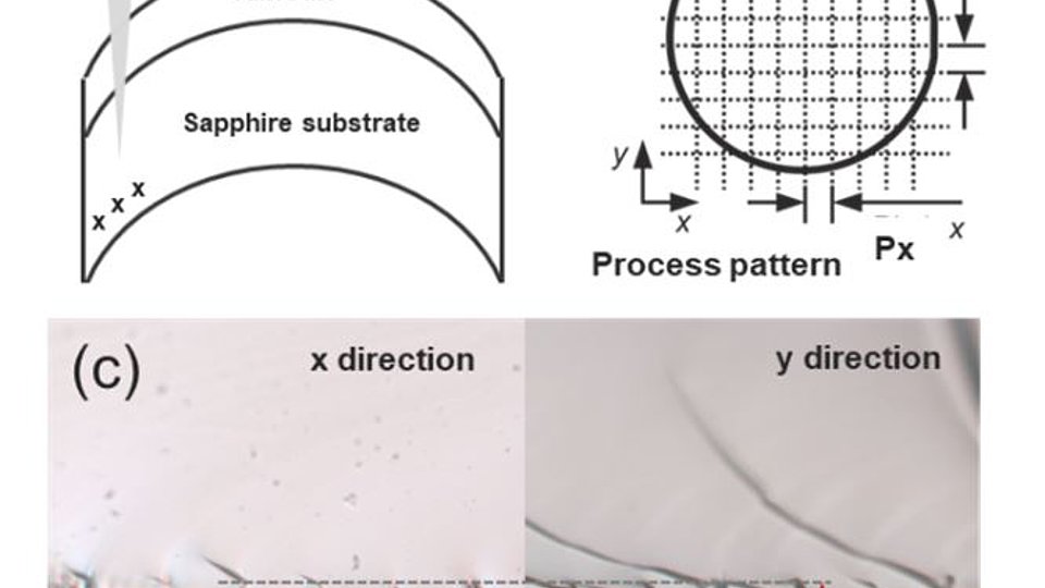
Fig. 1: (a) Process flow for bow reduction. (b) Wafer with process pattern. (c) Cross section view of processed wafers.
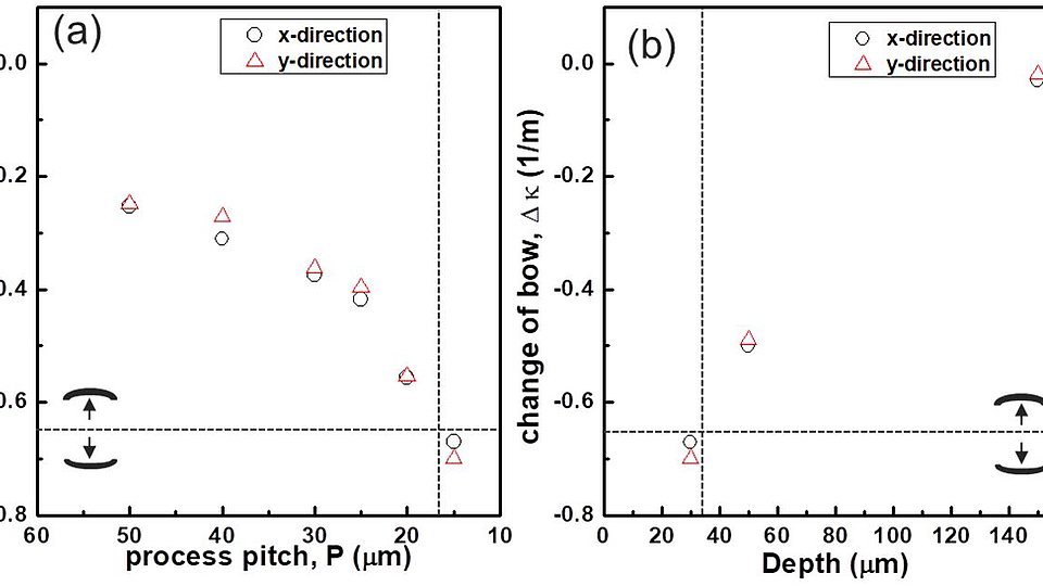
Fig. 2: Change of bow (a) versus inverse pitch (pattern depth 30 µm from sapphire backside), and (b) versus pattern depth (grid pitch 15 µm). Dashed lines: transition from a convex to a concave bow.
AlGaN-based deep-ultraviolet light-emitting diodes (DUV LEDs) are promising devices that could replace mercury discharge lamps in various applications. These include sterilization, water purification, medical diagnostics, phototherapy, and UV curing. AlGaN-based DUV LED heterostructures are usually realized on sapphire substrates. However, the large mismatch in thermal expansion coefficient between the group III nitride and sapphire substrate as well as lattice mismatches and extended defects in the epitaxial layers usually induce large residual stress and consequently a large wafer bow. During chip processing, the wafer bow can lead to a non-uniform thickness of deposited materials, non-uniform temperature profile or non-uniform etching depths across the wafers. Therefore, the bow should be well-controlled to minimize performance variations between devices on a wafer.
A laser patterning process that significantly reduces the wafer bow has been developed and qualified on 305 nm UVB LEDs. The process involves focusing a laser beam with 532 nm wavelength into the sapphire close to its back surface where it damages the crystal structures and induces stress. The parameters of the laser patterning were 160 mW, 40 kHz, 400 mm/s, and 15 ps for the average output power, pulse repetition frequency, stage speed and pulse duration, respectively. The laser beam was focused into the wafer from the heterostructure side. Fig. 1 shows the grid pattern written inside the sapphire. The laser induced stress was controlled by changing the pitch P of the scribe lines. Cross sectional views of the grid patterns created inside the sapphire substrate are shown in Fig. 1 (c). The vertical extension L of the damaged area in the sapphire was around 80 μm and started about 30 μm from the back surface of the sapphire.
Fig. 2 (a) shows the changes in radius of curvature (R) as function of the grid pitch for various laser-treated DUV LED wafers. After epitaxy, the radius of curvature of the convex bowed wafers along both x and y direction was about 1.4 m. The bow (κ = 1/R) of the wafers was gradually reduced by laser patterning when decreasing the pitch of the laser lines from 200 to 15 μm. After laser patterning with a grid pitch of about 20 µm, the direction of the bow changed from convex to concave. The change of bow (Δκ = κafter – κbefore) as a function of the pitch of the laser lines and their depth in the sapphire is shown in Fig. 2 (a) and (b), respectively. Here, the depth is defined as the distance of the lower end of the damaged area from the sapphire back surface. It is found that both the pitch of the lines and the position of the lines in the sapphire determine the wafer bow. Compressive stress is also induced in the AlGaN epilayers grown on the sapphire substrate, particularly due to the thermal expansion difference between the AlGaN and sapphire. Since the laser-induced compressive stress is implemented near the back surface of the sapphire substrate, it counterbalances the compressive stress generated by the AlGaN on the front surface of the sapphire.
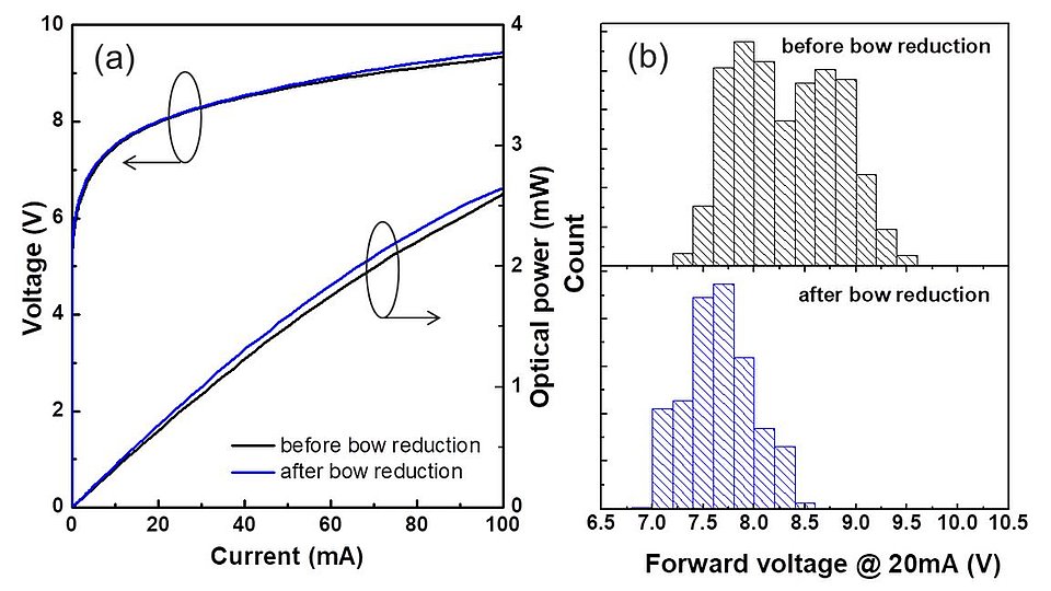
Fig. 3(a) and (b) shows the corresponding light output-current-voltage (L-I-V) characteristics and histograms of the forward voltages (at 20 mA) of LEDs with and without bow reduction. The electro-optical characteristics of the LEDs were not significantly affected by laser patterning. At the same time, the uniformity of LED operation voltage across the wafer was improved due to the bow reduction. This effect is attributed to a more uniform temperature distribution during contact annealing across the wafers with reduced bow. A reduced bow leads to a more uniform thermal coupling of the wafer to the heated susceptor during contact annealing. Since the contact resistivity strongly depends on the annealing temperature, the more uniform thermal coupling results in a more uniform operation voltage across the wafer.
Publication
Hyun Kyong Cho, Alex Külberg, Neysha Lobo Ploch, Jens Rass, Jan Ruschel, Tim Kolbe, Arne Knauer, Andreas Braun, Olaf Krüger, Sven Einfeldt, Markus Weyers, Michael Kneissl" Bow reduction of AlInGaN-based deep UV LED wafers using focused laser patterning", IEEE Photonics Technology Letters 30, 1792 (2018).


