Chip-integrated solution based on diamond NV centers – enabling compact magnetic field cameras with simplified measuring principle
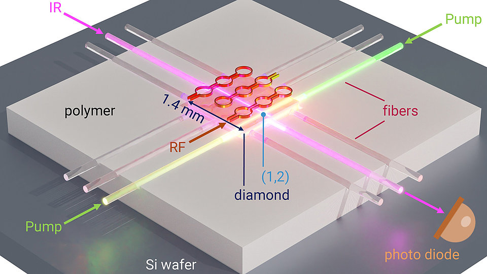
Fig. 1: Chip-integrated magnetic field multi-pixel sensor setup. The diamond substrate is embedded in the polymer-on-silicon platform. Fibers interfacing the diamond at either side deliver 532 nm pump and 1042 nm infrared light for infrared transmission measurements. Beam intersections define the sensor pixels (i,j). Exemplarily, pixel (1,2) is addressed in the image. Microwave inductor lines (RF) drive NV spin-flip transitions for IRA-ODMR.
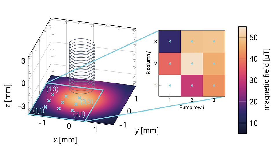
Fig. 2: A solenoid coil (gray spiral) located above pixel (3,3) generates a magnetic field. Its simulated magnetic field’s absolute value is depicted color-coded. The inset displays the magnetic field measured with the multi-pixel sensor. Pixel (1,1) is excluded due to an insufficient signal-to-noise ratio.
To date, ‘cameras’ to record images of weak magnetic fields are complex and expensive. Often, they operate at cryogenic temperatures or involve moving components to scan across a sample. This renders their integration into hand-held devices impossible. Magnetic field cameras possess relevance in medical diagnostics, like magnetoencephalography, as well as in life science research to gain insights into neural processes. This includes the long-desired research goal to record ‘movies’ of action potentials propagating through nerves [1].
We have developed, together with the Fraunhofer Heinrich Hertz Institute (HHI), a novel, fully fiber-packaged, mobile quantum sensor operating at ambient conditions to image magnetic fields and to spatially resolve 2D magnetic field gradients. The sensor employs a 1.4 × 1.4 × 0.2 mm³ diamond substrate containing nitrogen vacancy (NV) centers, which is embedded in a polymer-on-silicon platform. A matrix of magnetic field-sensitive pixels is defined within the diamond substrate by green pump laser beams at a wavelength of 532 nm, intersecting perpendicularly with infrared laser beams at a wavelength of 1042 nm (Fig. 1). Individual pixels (i,j) are addressed by activating the pump beam in row i and the infrared beam in column j. Active pixels absorb infrared light depending on the magnetic field to be probed and the frequency of a microwave field delivered to the pixels by microwave inductor lines (infrared absorption optically detected magnetic resonance, IRA-ODMR) [2]. Thus, the infrared absorption within the individual pixels is measured with a photo diode to derive the local magnetic field at each pixel. Subsequent readout of all pixels enables magnetic field imaging.
To demonstrate the multi-pixel sensor’s potential, we place a current-driven solenoid coil above pixel (3,3). The coil generates a magnetic field, which we simulate and record with our sensor (Fig. 2). The measured field is highest around pixel (3,3), where the coil is located. Moving away from this pixel, the measured field decays in accordance with the coil’s simulated field. Comparing the measured with the simulated magnetic field allows to retrieve the sensor position relative to the coil (blue crosses in Fig. 2 denote the retrieved sensor pixel positions). The close match between the experimental configuration and the reconstructed sensor position proves the sensor’s capability to localize magnetic objects.
In the future, the sensor will be integrated into a wearable device, which can be attached to the skin. We foresee applications for the magnetic field camera not only in medical diagnostics but also in lab-on-a-chip devices to discover drugs [3]. Furthermore, the sensor can be integrated into lithium ion batteries to monitor them and develop them further [4] as demanded by sustainable electromobility.
This project is funded by the German Federal Ministry of Education and Research (BMBF) within the ‘DiNOQuant’ project (No. 13N14921), by the European Research Council within the ERC Starting Grant ‘QUREP’ (No. 851810), and by the Einstein Research Unit ‘Perspectives of a quantum digital transformation: Near-term quantum computational devices and quantum processors’.
Publications
- J. M. Bopp, H. Conradi, F. Perona, A. Palaci, J. Wollenberg, T. Flisgen, A. Liero, H. Christopher, N. Keil, W. Knolle, A. Knigge, W. Heinrich, M. Kleinert, T. Schröder, ‘Diamond-on-chip infrared absorption magnetic field camera’, arXiv:2401.00854 (2023).
- T. Schröder, F. Perona, J. M. Bopp, M. Kleinert, H. Conradi, US patent US11719765B2 (2023), EU patent application EP4099041A1 (2021).
References
[1] J. L. Webb et al., Sci. Rep. 11, 2412 (2021)
[2] V. M. Acosta et al., Appl. Phys. Lett. 97, 174104 (2010)
[3] R. D. Allert et al., Lab Chip 22, 4831–4840 (2022)
[4] M. G. Bason et al., J. Power Sources 533, 231312 (2022)

