Power Electronic Devices with Wide-Bandgap Semiconductors
We have developed a GaN device process for power-electronic transistors and half-bridges and operate a process technology for normally-off 650 V GaN switching transistors.
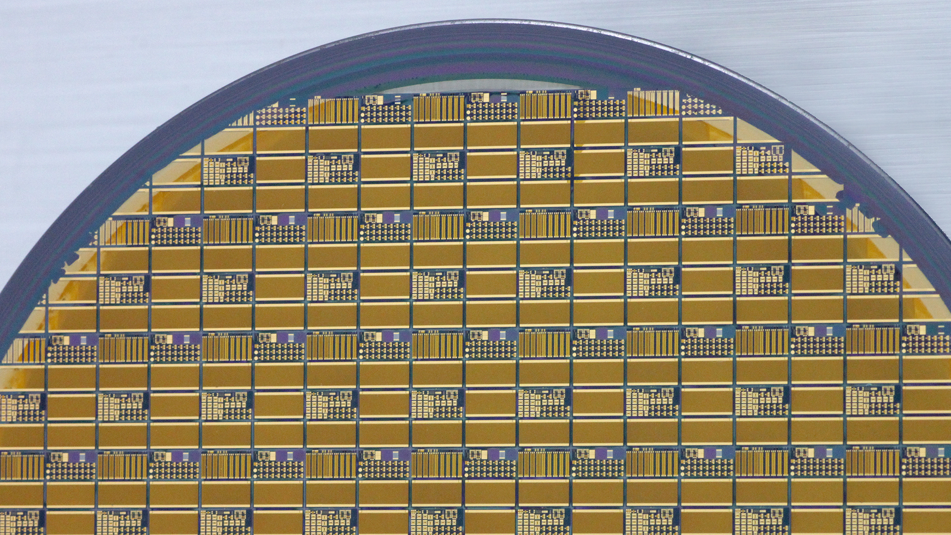
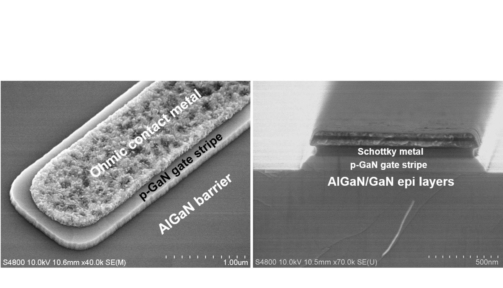
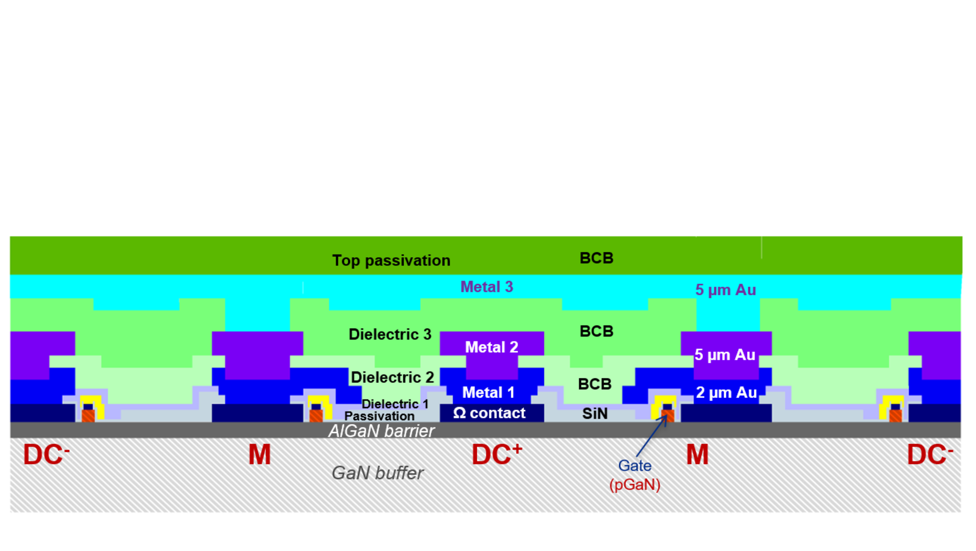
A p-GaN gate module converts the intrinsically normally-on GaN transistors into normally-off devices.We use p-GaN gates with ohmic gate contacts or with Schottky-type gate contacts. The transistors are processed on 4" GaN-on-Si or GaN-on-SiC wafers using i-line stepper lithography. The largest transistors in the 650 V class have around 60 mOhm on-state resistance and switch currents of typically 10-20 A.
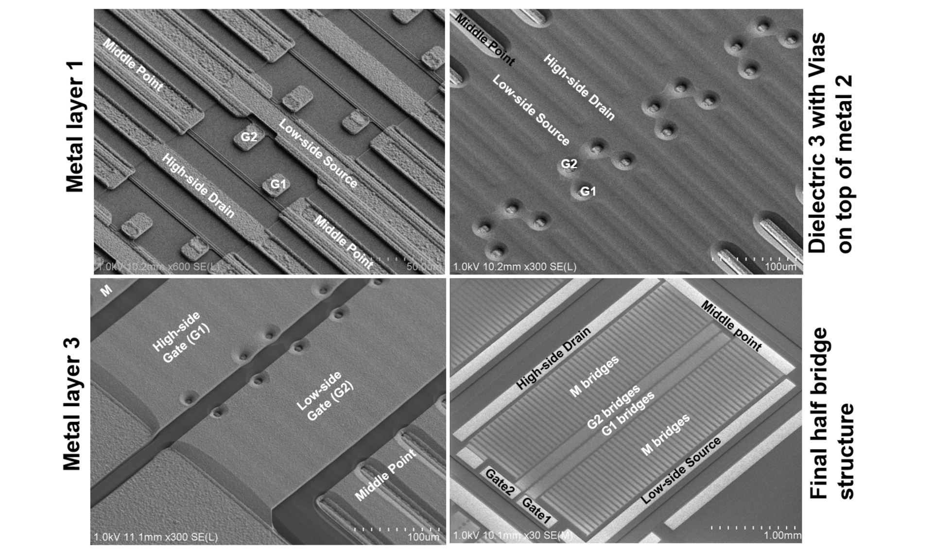
In addition to discrete switching transistors, two high-current metal layers of 5 µm thick electro-plated gold enable monolithic integration of particularly compact half-bridge structures. We use benzocyclobutene (BCB) as a high-voltage-resistant dielectric, which we also use for the final encapsulation of the GaN chips. Vias in the SiN and BCB layers electrically connect the individual metal layers.
This technology platform also forms the basis for the development of AlN-based transistor technology for voltages up to 1200 V.